Wide range core supply compatible level shifter circuit

a technology of wide range core supply and level shifter, which is applied in logic circuits, power consumption reduction, pulse automatic control, etc., can solve the problems of increasing the footprint of the circuit, reducing the frequency of operation, and reducing the possibility of devices even failing to function

Active Publication Date: 2015-11-03
STMICROELECTRONICS INT NV
View PDF7 Cites 3 Cited by
  • Summary
  • Abstract
  • Description
  • Claims
  • Application Information

AI Technical Summary

Benefits of technology

[0006]The level shifter circuit disclosed herein is capable of reducing the threshold voltage of the MOS devices without introducing additional control circuitry. Instead, the level shifter circuit is redesigned so the transistors can sense a broader range of low supply voltages and can operate at a very high frequency. A preferred circuit design disclosed herein uses dual gate transistors implemented with fully depleted silicon-on-insulator (FDSOI) technology. Lowering the Vt can be accomplished through dynamic secondary gate control in which a back-biasing technique is used to operate the dual-gate FDSOI NMOS transistors with enhanced switching performance. By coupling both primary and secondary gates of the dual-gate FDSOI NMOS devices together, the threshold voltage of the device is lowered during the transition from the off state to the on state, by enhancing the amount of charge required to form an inversion region in the channel of the transistor. Meanwhile, conventional DC conditions are maintained during steady state operation. Consequently, the MOS devices can operate at very low core voltage supply levels, down to as low as 0.4 V, which allows the transistors to respond quickly and to switch at higher speeds. Such high performance NMOS devices run on a much wider range of power supplies and can operate at higher frequencies. Because no components are added, the inventive level shifting circuits are more area efficient.

Problems solved by technology

In addition, at lower core voltages, if the MOS device does turn on, the transition from the off state to the on state occurs slowly, and thus the frequency of operation is reduced, or the device may even fail to function.
However, conventional solutions have relied on the introduction of additional control circuitry into the level shifting circuit, which tends to increase the footprint of the circuit on an IC chip.

Method used


Image

  • Wide range core supply compatible level shifter circuit
  • Wide range core supply compatible level shifter circuit
  • Wide range core supply compatible level shifter circuit

Examples


Embodiment Construction

[0018]In the following description, certain specific details are set forth in order to provide a thorough understanding of various disclosed embodiments. However, one skilled in the relevant art will recognize that embodiments may be practiced without one or more of these specific details, or with other methods, components, materials, etc. In other instances, well-known structures associated with NMOS and PMOS transistors and associated circuits have not been shown or described in detail to avoid unnecessarily obscuring descriptions of the embodiments.

[0019]Unless the context requires otherwise, throughout the specification and claims which follow, the word “comprise” and variations thereof, such as, “comprises” and “comprising” are to be construed in an open, inclusive sense, that is as “including, but not limited to.”

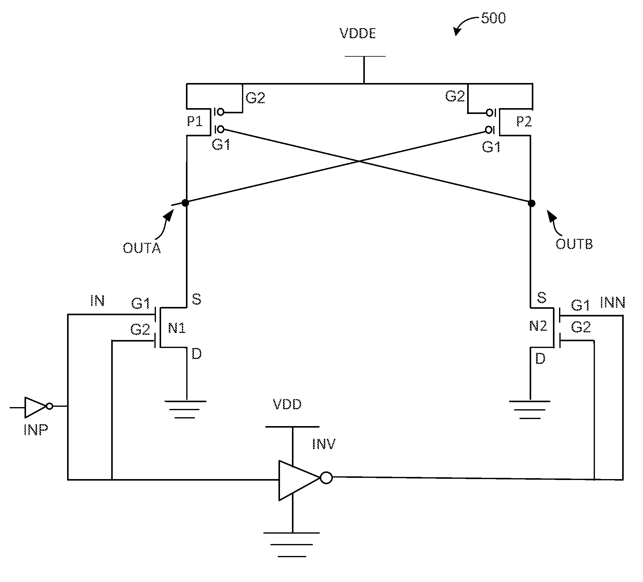
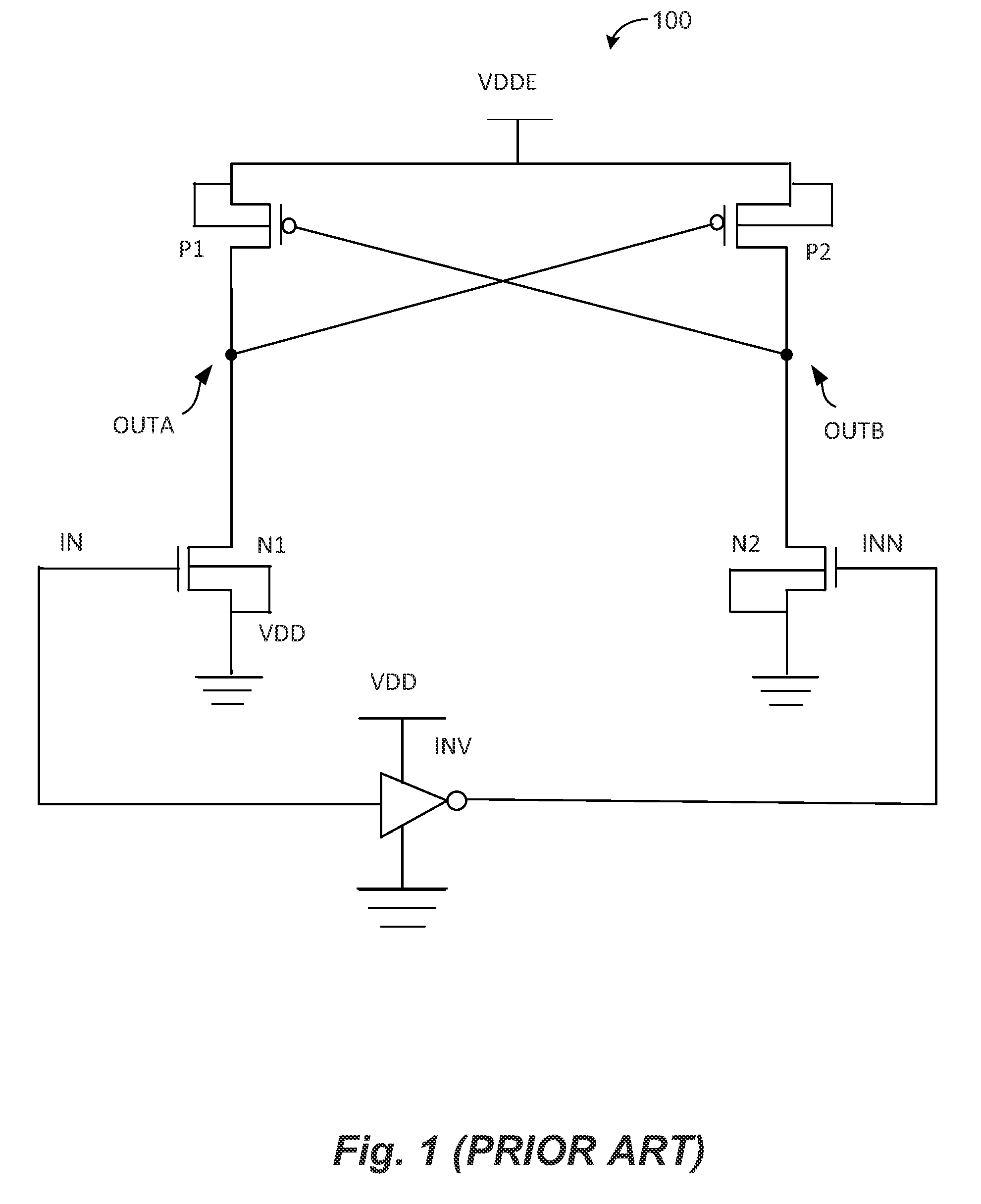
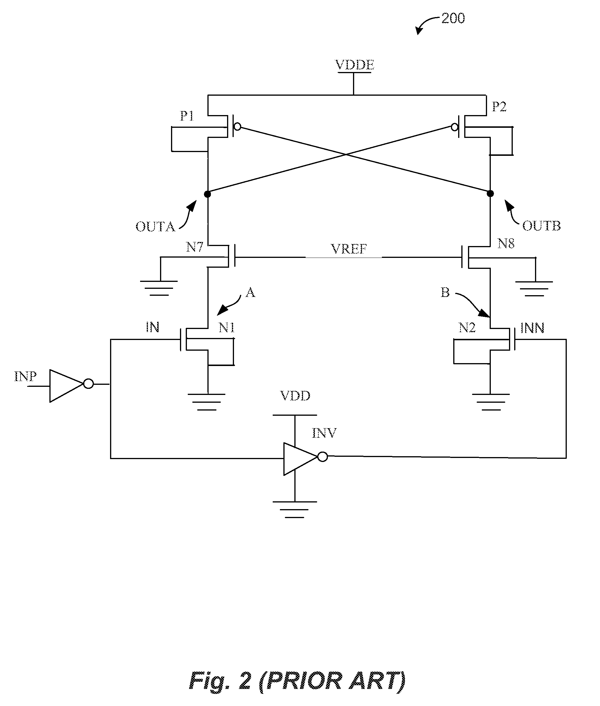
[0020]FIG. 1 shows a first conventional level shifter circuit 100 that receives an input signal IN or INN at a low voltage level, VDD, and generates an output signal ...


PUM


Abstract

A level shifter circuit is implemented with dual gate fully depleted silicon-on-insulator (FDSOI) technology. By enhancing the performance of the NMOS and devices within the level shifting circuit, the Vt of the dual gate FDSOI NMOS transistors is lowered without a need for additional control circuitry. Lowering the Vt can be accomplished through dynamic secondary gate control, by coupling together primary and secondary gates of the NMOS devices, while secondary gates of the PMOS devices can be coupled to a high voltage supply level. Such high performance NMOS devices can then operate at higher frequencies and run on a much wider range of core power supplies. Meanwhile, conventional DC conditions are maintained during steady state operation. Because no components are added to the level shifter circuit, the higher performance is achieved without an increase in size and current consumption.

Description

BACKGROUND[0001]1. Technical Field[0002]The present disclosure generally relates to the design of integrated level shifter circuits that are operable at more than one power supply voltage.[0003]2. Description of the Related Art[0004]Some integrated circuits (ICs) are designed to operate at two different supply voltages—a first supply voltage for core functions, and a second supply voltage for interfacing functions. Typically, the second supply voltage is higher than the first supply voltage, because interface circuits normally operate at a higher voltage level than the core of the IC. A higher supply voltage level at the I / O pads is desirable to drive large electrical loads at optimum speed. A lower voltage supply level at the core enables use of advanced transistors that have thinner gate oxide. For such ICs to be used in, and to communicate with, external systems whose power supply voltages are higher, there is a need for voltage level matching by input-output (I / O) interface circ...

Claims


Application Information

Patent Timeline
Patent Type & Authority Patents(United States)
IPC IPC(8): H03L5/00H03K19/0185H03K19/00H03K19/017
CPCH03K19/0185H03K19/0013H03K19/017H03K3/356113
Inventor AGRAWAL, ANKIT
Owner STMICROELECTRONICS INT NV
Why Eureka
Try Eureka