Silicon-based electro-optic device

an electro-optic device and silicon-based technology, applied in the field of electro-optic devices, can solve the problems of inability to achieve an efficient optical connection for such an optical modulator, the low cost of high-speed operation and the inability to reduce the loss of optical propagation in the optical modulator, etc., to achieve the effect of reducing power consumption, reducing current density, and reducing costs

Active Publication Date: 2011-09-01
ADVANCED MICRO FOUNDRY PTE LTD +1
View PDF7 Cites 50 Cited by
  • Summary
  • Abstract
  • Description
  • Claims
  • Application Information

AI Technical Summary

Benefits of technology

[0019]As one of silicon-based electro-optic devices that can be integrated on a silicon (Si) semiconductor substrate, the optical modulator based on the carrier plasma effect can realize, in a very small size of submicron order, a reduction in costs, reduction of current density, reduction of power consumption, a high modulation degree, driving at a reduced voltage and high speed modulation. However, as described above, it is difficult to achieve an efficient optical connection for such an optical modulator based on the carrier plasma effect by adjusting the arrangement of the electrode contact layer. Furthermore, a manner of arranging the electrode contact layer which enables both the high-speed operation and a reduction in optical propagation loss in the optical modulator is unknown.
[0020]An electrode connection structure which achieves an efficient optical connection and which enables both high-speed operations and a reduction in optical propagation loss has been demanded in a silicon-based optical modulator formed on an SOI substrate.

Problems solved by technology

However, as described above, it is difficult to achieve an efficient optical connection for such an optical modulator based on the carrier plasma effect by adjusting the arrangement of the electrode contact layer.
Furthermore, a manner of arranging the electrode contact layer which enables both the high-speed operation and a reduction in optical propagation loss in the optical modulator is unknown.

Method used


Image

  • Silicon-based electro-optic device
  • Silicon-based electro-optic device
  • Silicon-based electro-optic device

Examples


Embodiment Construction

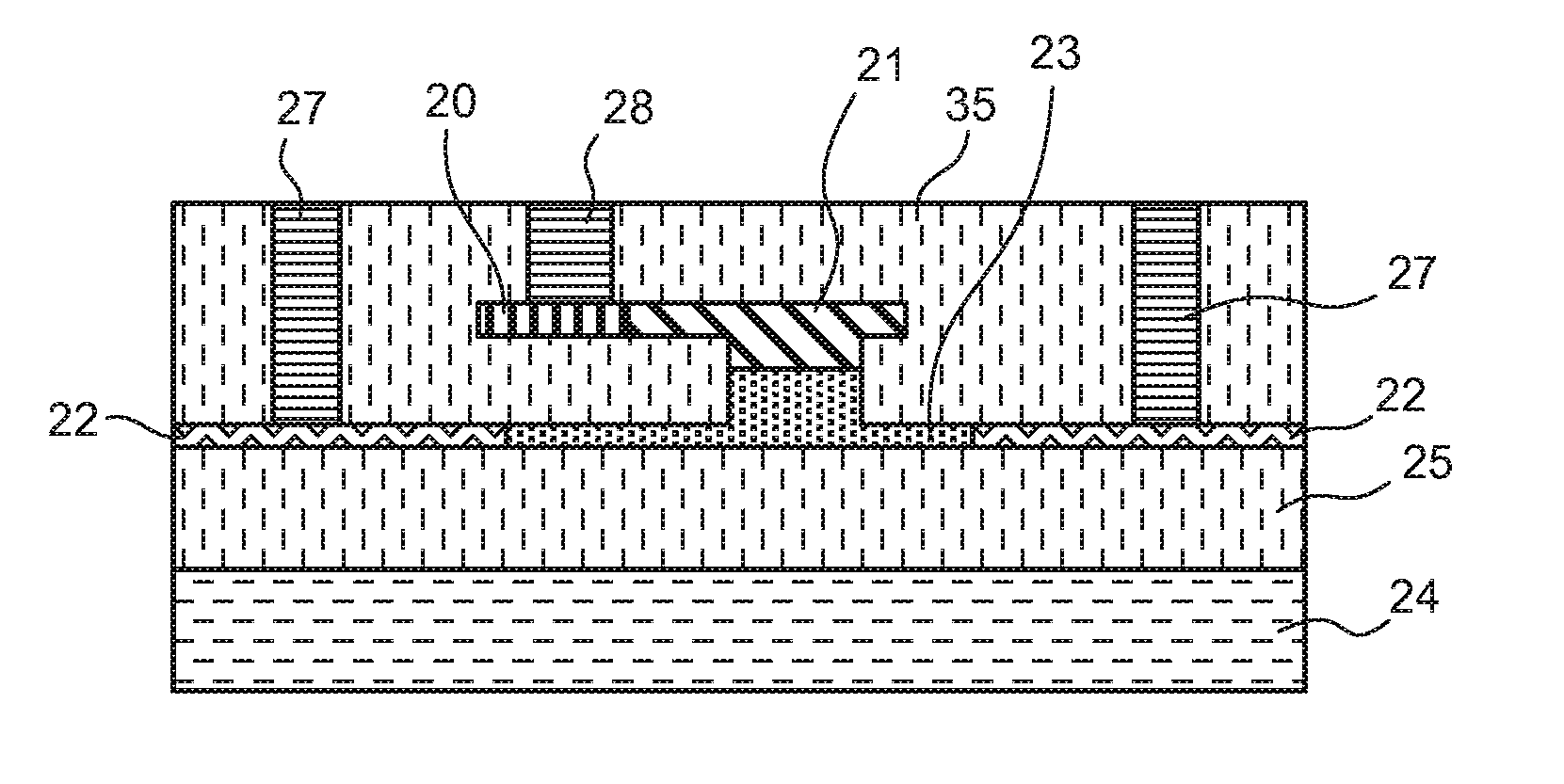
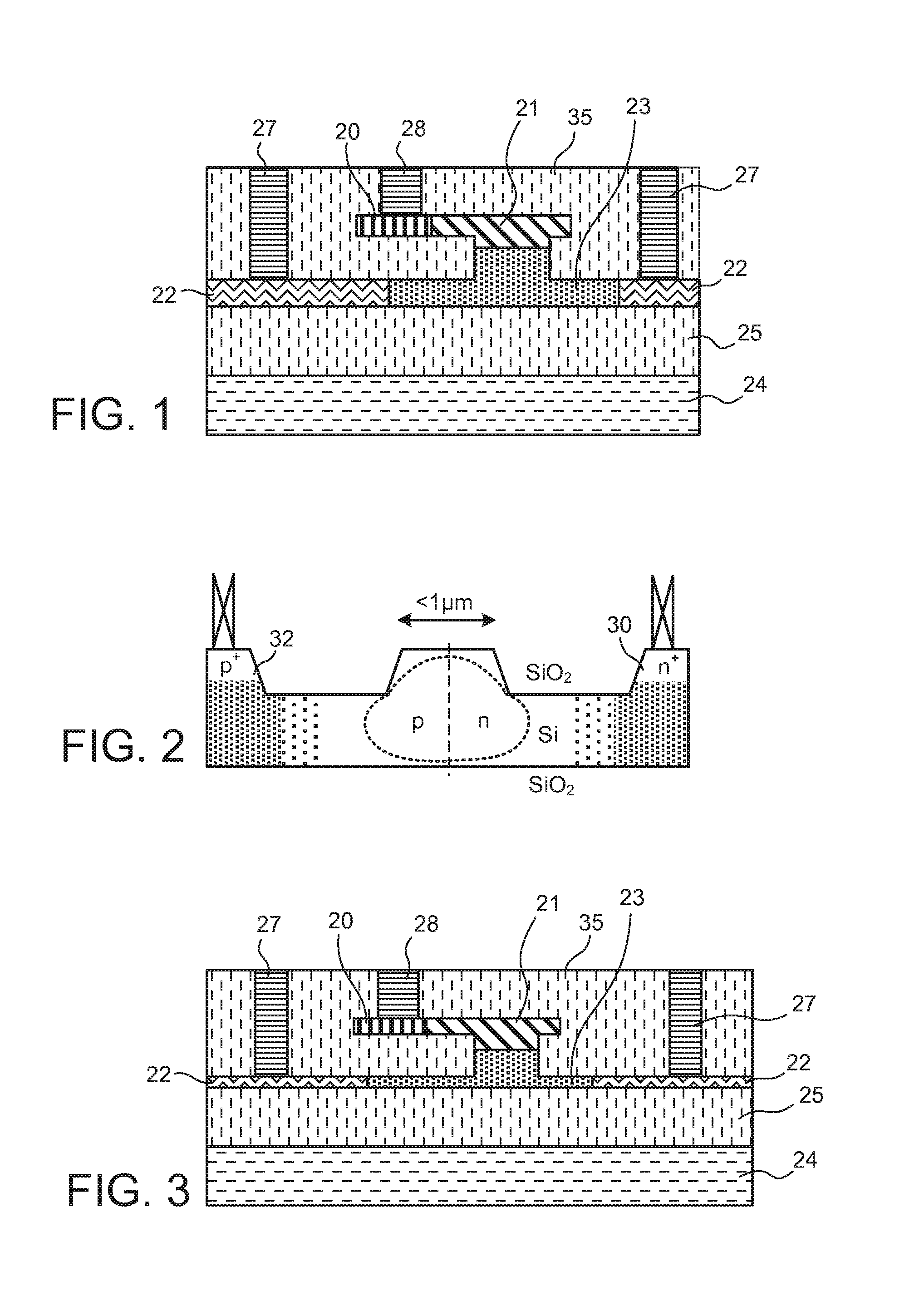
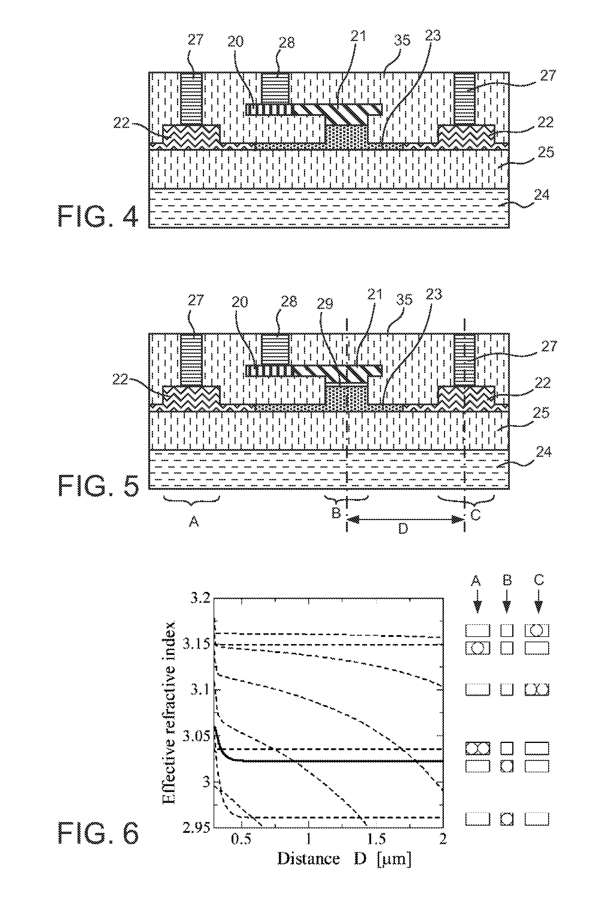
[0031]Before description of exemplary embodiments, a portion of a rib waveguide where a slab is connected to an electrode structure will be described.

[0032]To allow the refractive index of a silicon waveguide to be changed using the carrier plasma effect, an external voltage needs to be applied to a core portion of the waveguide. To achieve this, an electrode is connected to a portion of the rib waveguide which extends from a slab. Metal such as aluminum (Al) or copper (Cu) is generally used as the electrode. The portion extending from the slab and connected to the electrode is configured with a silicon layer doped with impurities of a high concentration, so as to serve as a contact layer. The portion in which the contact layer and the metal electrode are connected together is configured with a silicide layer to allow the electrode and the contact layer to be reliably electrically connected together.

[0033]FIG. 3 shows an electro-optic device which is similar to the device shown in F...


PUM

PropertyMeasurementUnit
thicknessaaaaaaaaaa
thicknessaaaaaaaaaa
distanceaaaaaaaaaa

Abstract

In an electro-optic device, a stack structure including a first silicon layer of a first conductivity type and a second silicon layer of a second conductivity type has a rib waveguide shape so as to form an optical confinement area, and a slab portion of a rib waveguide includes an area to which a metal electrode is connected. The slab portion in the area to which the metal electrode is connected is thicker than a surrounding slab portion. The area to which the metal electrode is connected is set so that a range of a distance from the rib waveguide to the area to which the metal electrode is connected is such that when the distance is changed, an effective refractive index of the rib waveguide in a zeroth-order mode does not change.

Description

[0001]This application is based upon and claims the benefit of priority from Singapore patent application No. 201001336-5, filed on Mar. 1, 2010, the disclosure of which is incorporated herein in its entirety by reference.BACKGROUND OF THE INVENTION[0002]1. Field of the Invention[0003]The present invention relates to an electro-optic device formed on a silicon platform and utilized in the field of, for example, optical communication, and in particular, to a silicon-based electro-optic device formed on an SOI (Silicon-On-Insulator) substrate.[0004]2. Description of the Related Arts[0005]Information communication networks typified by the Internet are constructed so as to spread throughout the world as social infrastructure essential for peoples' lives. Optical communication using optical fibers is a technique to support huge traffics on the Internet. Optical communication devices using silicon platforms can utilize a 1.3-μm band and a 1.55-μm band of wavelengths, which are included in...

Claims


Application Information

Patent Timeline
Patent Type & Authority Applications(United States)
IPC IPC(8): G02F1/025
CPCG02F1/025G02F2201/066G02F2202/105G02F2202/06G02F2201/12
Inventor USHIDA, JUNFUJIKATA, JUNICHIYU, MING-BINDING, LIANGZHU, SHIYANG
Owner ADVANCED MICRO FOUNDRY PTE LTD
Why Eureka
Try Eureka