Transmission electron microscope having electron spectrometer

a technology of electron microscope and electron beam, which is applied in the field of electron microscope, can solve the problems of weak chemical shift, deterioration of device characteristics and reliability, and drift of accelerating voltage of electron beam, and achieve the effect of high efficiency, high accuracy and efficient correction of distortion

Inactive Publication Date: 2011-10-06
HITACHI HIGH-TECH CORP
View PDF15 Cites 5 Cited by
  • Summary
  • Abstract
  • Description
  • Claims
  • Application Information

AI Technical Summary

Benefits of technology

[0015]According to the method and apparatus for correcting distortion in a spectral image of the present invention, the distortion in the spectral image of a sample to be analyzed can be corrected with high efficiency and high accuracy by comparing a two-dimensional electron beam position image formed by two orthogonal axes consisting of an axis of the amount of

Problems solved by technology

As silicon semiconductors, magnetic devices, and so on have been manufactured in ever decreasing sizes and with ever increasing scales of integration, deteriorations of the device characteristics and reliability decrease have become greater issues.
In the case of this technique, however, drift of the accelerating voltage of the electron beam caused by variations in external dist

Method used


Image

  • Transmission electron microscope having electron spectrometer
  • Transmission electron microscope having electron spectrometer
  • Transmission electron microscope having electron spectrometer

Examples


Embodiment Construction

[0032]Embodiments of the present invention are hereinafter described in detail with reference to the drawings. In all the figures for illustrating the embodiments, identical members are in principle indicated by the same symbols. Their repeated description is omitted.

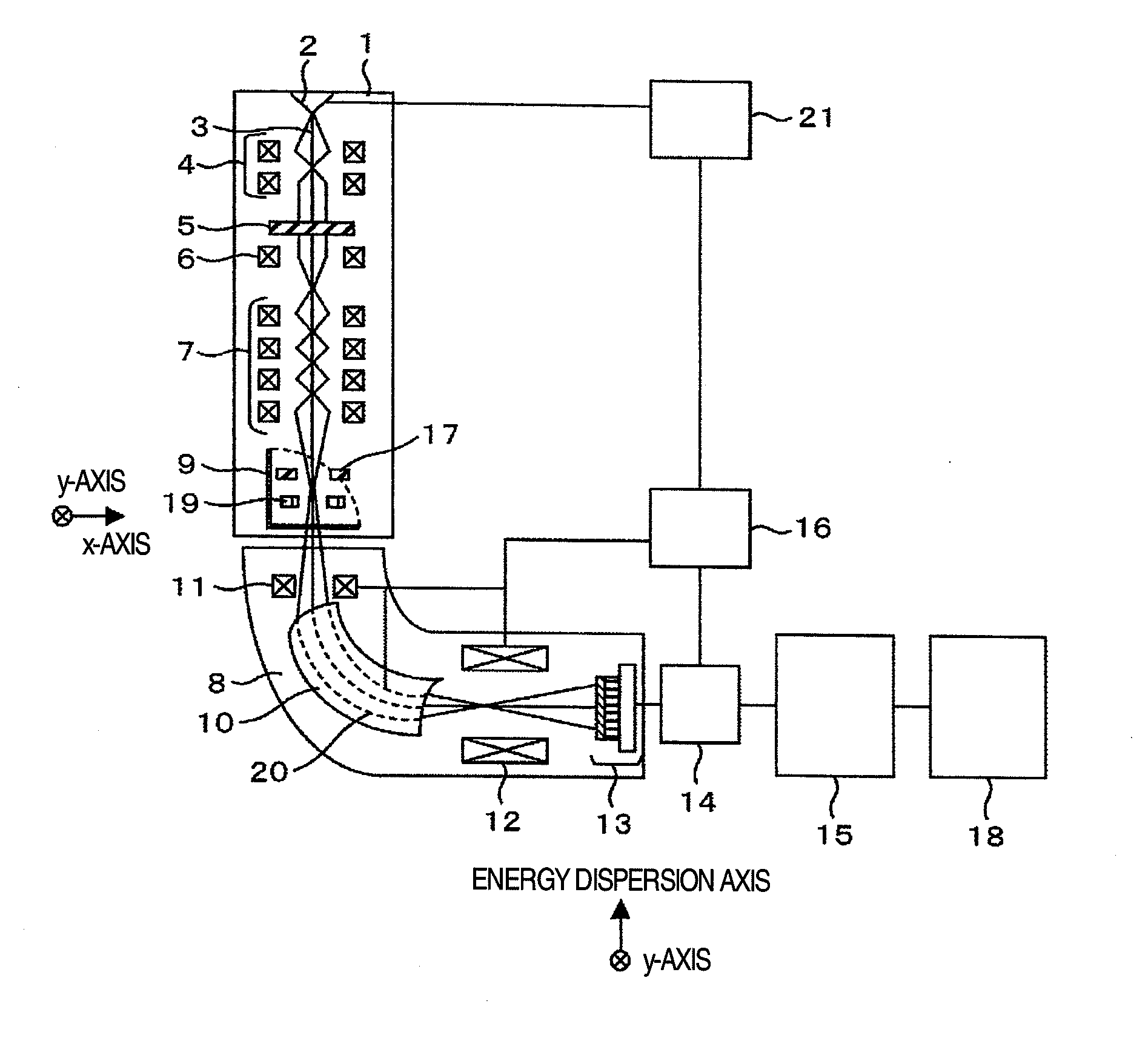
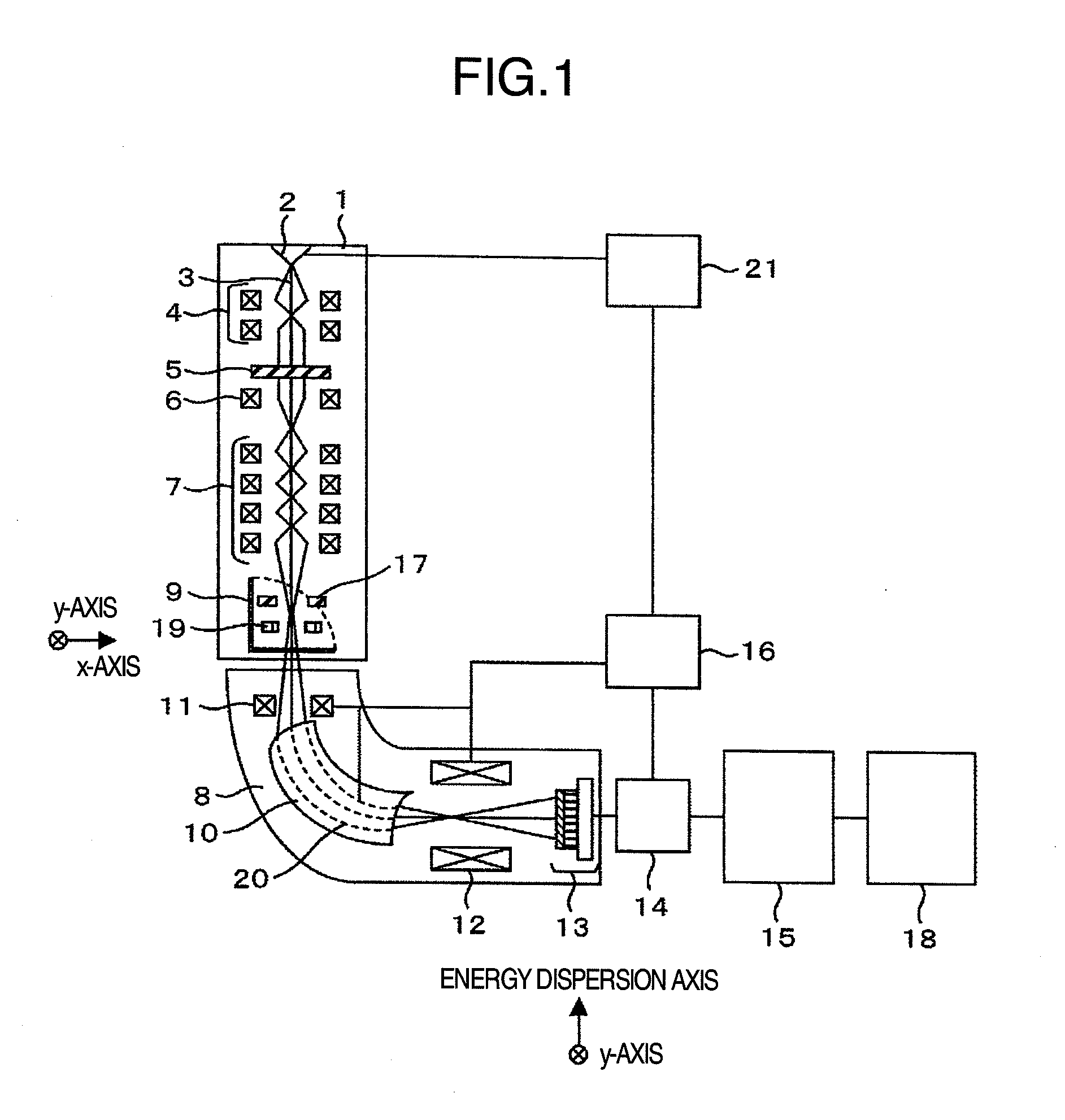
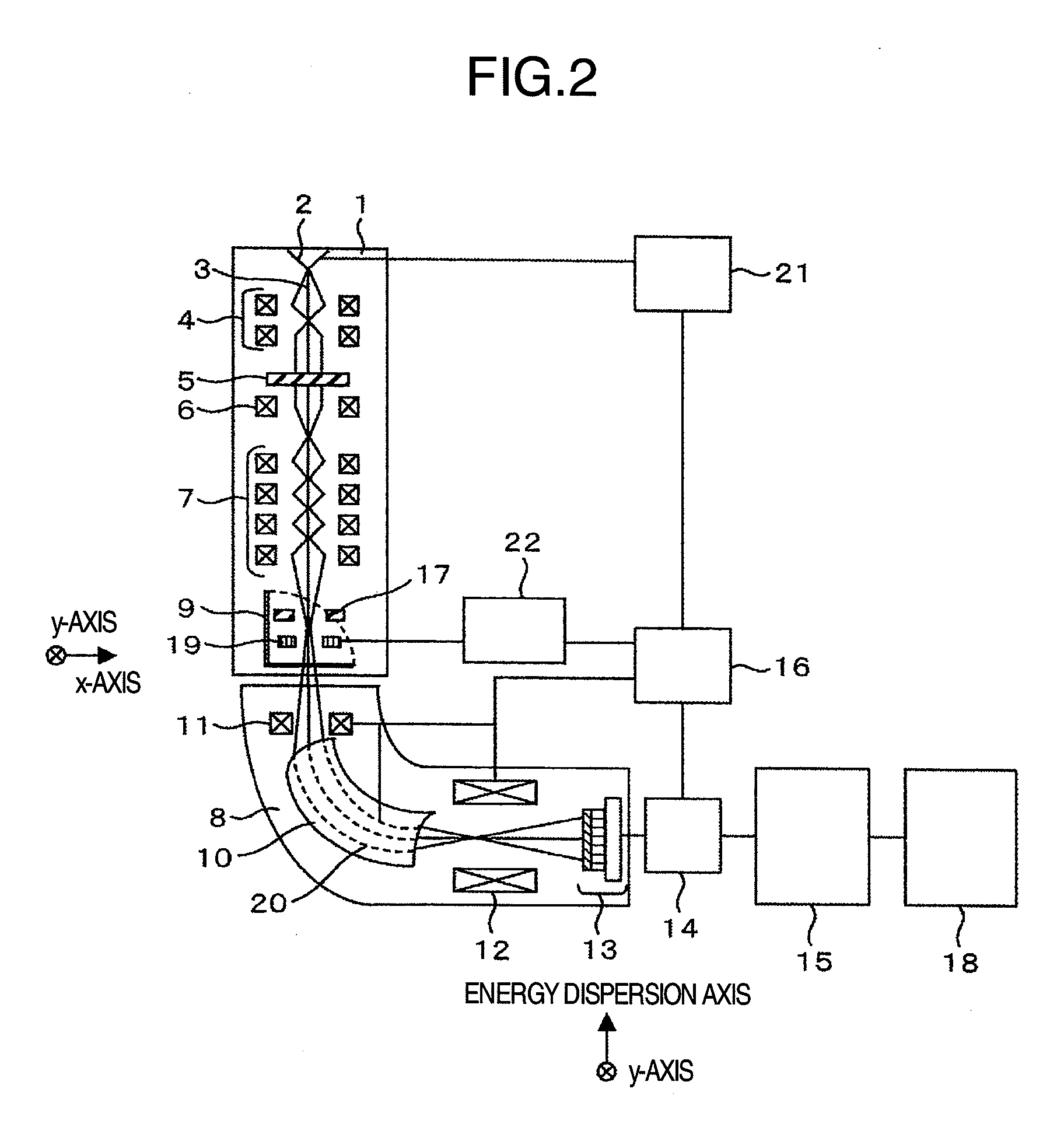
[0033]FIG. 1 is a schematic diagram showing one example of a transmission electron microscope equipped with an electron spectrometer being one embodiment according to the present invention.

[0034]The transmission electron microscope equipped with the electron spectrometer of the present embodiment is composed of a transmission electron microscope 1, the electron spectrometer 8, an image display device 14, a central control unit 16, a spectral image distortion correction apparatus 15, and others. The transmission electron microscope 1 has an electron source 2 emitting an electron beam 3, condenser lenses 4, an objective lens 6, an imaging lens system 7, a fluorescent screen 9, and so on. A sample 5 is disposed between the...


PUM


Abstract

In a spectral image formed by two orthogonal axes, one of which is an axis of the amount of energy loss and the other of which is an axis of positional information, by the use of an electron spectrometer and a transmission electron microscope, distortion in the spectral image of a sample to be analyzed is corrected with high efficiency and high accuracy by comparing electron beam positions calculated from a two-dimensional electron beam position image formed by the two orthogonal axes (the axis of the amount of energy loss and the axis of positional information) with reference electron beam positions, and calculating amounts of the distortion based on the differences of the electron beam positions. Method and apparatus are offered which correct distortion in a spectral image with high efficiency and high accuracy, the image being formed by the two orthogonal axes (the axis of the amount of energy loss and the axis of positional information).

Description

TECHNICAL FIELD[0001]The present invention relates to an electron microscope and, more particularly, to a transmission electron microscope having an electron spectrometer for spectrally dispersing an electron beam according to the amount of energy possessed by the beam.BACKGROUND ART[0002]As silicon semiconductors, magnetic devices, and so on have been manufactured in ever decreasing sizes and with ever increasing scales of integration, deteriorations of the device characteristics and reliability decrease have become greater issues. In recent years, in order to analyze defects in semiconductor devices in the nanometer regime and to locate and solve the causes of the defects in a fundamental manner in the course of development of novel processes and mass production, spectral analysis using (scanning) transmission electron microscopy ((S)TEM) and electron energy loss spectroscopy (EELS) and analysis of two-dimensional elemental distributions have become essential analytical means.[000...

Claims


Application Information

Patent Timeline
IPC IPC(8): G01N23/00H01J37/153
CPCH01J37/05H01J2237/2446H01J37/244H01J37/153
Inventor TERADA, SHOHEITANIGUCHI, YOSHIFUMIHIRANO, TATSUMI
Owner HITACHI HIGH-TECH CORP
Why Eureka
Try Eureka