Sense-Amplification With Offset Cancellation For Static Random Access Memories

a random access memory and offset cancellation technology, applied in the field of sense amplification with offset cancellation for static random access memories, can solve the problems of large embedded memory integration, increasing random variability, rough line edges, etc., and achieves the effects of shorter cell access time, higher data stability, and high sensitivity to the current of the sram cell curren

Inactive Publication Date: 2011-10-20
SACHDEV MANOJ +3
View PDF5 Cites 17 Cited by
  • Summary
  • Abstract
  • Description
  • Claims
  • Application Information

AI Technical Summary

Benefits of technology

[0006]A sense amplifier scheme which allows for the compensation of offsets. Compensating for offsets in sense amplifier circuits offers higher sensitivity to the SRAM cell current. Hence, the sense amplifier scheme allows for a shorter cell access time which results in a higher data stability and faster operation.

Problems solved by technology

While embedded memories are important performance enablers, they come with many challenges.
The difficulties in integrating large, dense embedded memories are primarily related to manufacturing.
While variability used to be primarily systematic, as feature sizes scale below 100 nm random variability has become increasingly problematic.
There are numerous causes of random variability, including sub-wavelength lithography, random dopant fluctuations, line edge roughness and negative bias temperature instability (NBTI).
Increasingly large embedded memories are being integrated into ICs, and as such the variability over the entire array can be very large.
If sufficiently large design margins are not used in the design phase, variability can result in failures.
If the amplifier has an intrinsic offset due to process variability then the size of the input signal will need to be large enough to compensate for that offset, or else an incorrect decision will be made.

Method used


Image

  • Sense-Amplification With Offset Cancellation For Static Random Access Memories
  • Sense-Amplification With Offset Cancellation For Static Random Access Memories
  • Sense-Amplification With Offset Cancellation For Static Random Access Memories

Examples


embodiment 400

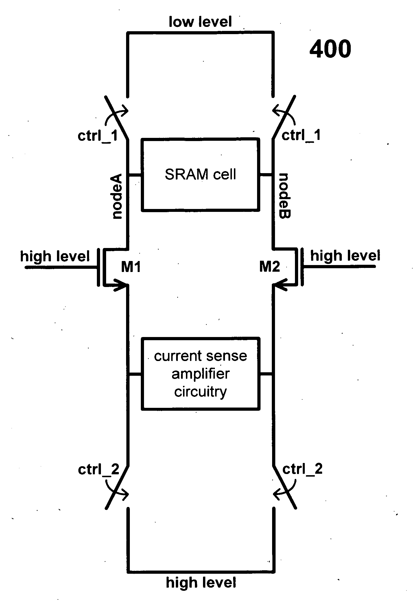
[0030]FIG. 5 is a circuit diagram showing the details of the embodiment 400. In this configuration the nodes nodeA and nodeB are commonly referred to as bitlines.

[0031]FIG. 6 shows the associated waveforms for the embodiment 400. During the read operation the bitlines develop a differential voltage. After a period of time the sense amplifier is enabled via a control signal SAE. Once the signal SAE is enabled the current sense amplifier turns on and amplifies the differential voltage on the bitlines to full swing.

[0032]FIG. 7 is a conceptual diagram showing one possible implementation where the offset cancellation scheme is utilized in conjunction with a voltage sense amplifier. The transistors of interest as labelled M1 and M2 and in this embodiment are NMOS transistors. This is a voltage sense amplifier as the sense amplifier senses the voltage at the gates of the transistors M1 and M2. During the offset cancellation stage the input to the transistors M1 and M2 is held at a high vo...

second embodiment

[0037]FIG. 10 is a circuit diagram showing the scheme 700 and it is denoted by the number 1000. In this configuration the nodes nodeA and nodeB are also the output nodes of the sense amplifier. Transistors M3 and M4 are multiplexing transistors which connect the sense amplifier to the SRAM cells via complementary signals known as bitlines (BL and BLB).

[0038]The gates of the NMOS transistors M1 and M2 need to remain at a high voltage level during the offset cancellation stage. The sense amplifier enable signal SAE is used to control the voltage level at the gates of transistors M1 and M2. During the offset cancellation stage the signal SAE is low and as such the input signals to the transistors M1 and M2 are held at a high voltage level via transistors M5 and M6. Moreover, the signal SAE is low thus transistors M3 and M4 are off, blocking the signals BL and BLB. During the offset cancellation stage first the signal ctrl_1 is enabled. This turns on transistors M7 and M8, thus connecti...

embodiment 1000

[0040]The waveforms in FIG. 9 are also applicable to embodiment 1000.

[0041]FIG. 11 is a conceptual diagram denoted by the number 1100 showing one possible implementation where the offset cancellation scheme is utilized in conjunction with a voltage sense amplifier. The transistors of interest as labelled M1 and M2 and in this embodiment are PMOS transistors. This is a voltage sense amplifier as the sense amplifier senses the voltage at the gates of the transistors M1 and M2. During the offset cancellation stage the input to the transistors M1 and M2 is held at a low voltage level in order that they remain on. During the offset cancellation stage the transistors M3 and M4 are off in order to isolate the sense amplifier from the bitlines. When the signal ctrl_1 is enabled the nodes nodeA and nodeB are connected to a high voltage level through the transistors M1 and M2. M1 and M2 are PMOS transistors and as such nodes nodeA and nodeB are able to reach the high voltage level. When the s...


PUM


Abstract

An offset cancellation scheme for sense amplification is described. The scheme consists of group of transistors which are selectively coupled to high and low voltage levels via multi-phase timing. This results in a voltage level on nodes of interest which are a function of transistor mismatch. The resulting voltage levels act to compensates for the transistor mismatch, thereby improving the reliability of the sense amplifier in the presence of process non-idealities. The offset cancellation scheme is applicable to numerous types of sense amplifiers.

Description

[0001]An offset cancellation scheme for sense amplification is described. The offset cancellation scheme is applicable to numerous types of sense amplifiers and is enabled with a multi-phase timing scheme. This application claims the benefit of priority of U.S. Provisional Patent Application No. 61 / 202,805 filed Apr. 8, 2009 which is incorporated herein by reference in its entirety.BACKGROUND OF THE INVENTION[0002]Embedded memories are critical blocks in modern system-on-chip (SOC) integrated circuit. On many modern integrated circuits embedded memory arrays consume more than half of the die area. The penalty in terms of latency resulting from an off-chip memory access makes it desirable to include on-chip caches which are as large as possible. As CMOS technology scale deep into the nanometric regime the density of bitcells has significantly increased, resulting in much larger embedded memory for the same die area.[0003]While embedded memories are important performance enablers, the...

Claims


Application Information

Patent Timeline
Patent Type & Authority Applications(United States)
IPC IPC(8): G11C7/06H03F3/16
CPCG11C7/062G11C2207/104G11C2207/063
Inventor SACHDEV, MANOJSHARIFKHANI, MOHAMMADSHAH, JASPAL SINGHRENNIE, DAVID
Owner SACHDEV MANOJ
Why Eureka
Try Eureka