
Optical transceivers for use in fiber optic communication networks

a technology of optical transceivers and fiber optic communication networks, applied in the direction of multi-channel sub-channel allocation, polarisation multiplex systems, multi-channel communication, etc., can solve the problems of reduced optical unregenerated reach, high power consumption associated with digital signal processing (dsp) algorithms, and reduce circuit size and power consumption. , the effect of simplifying the above dsp algorithms

Active Publication Date: 2011-10-20
CIENA
View PDF19 Cites 153 Cited by
  • Summary
  • Abstract
  • Description
  • Claims
  • Application Information

AI Technical Summary

Benefits of technology

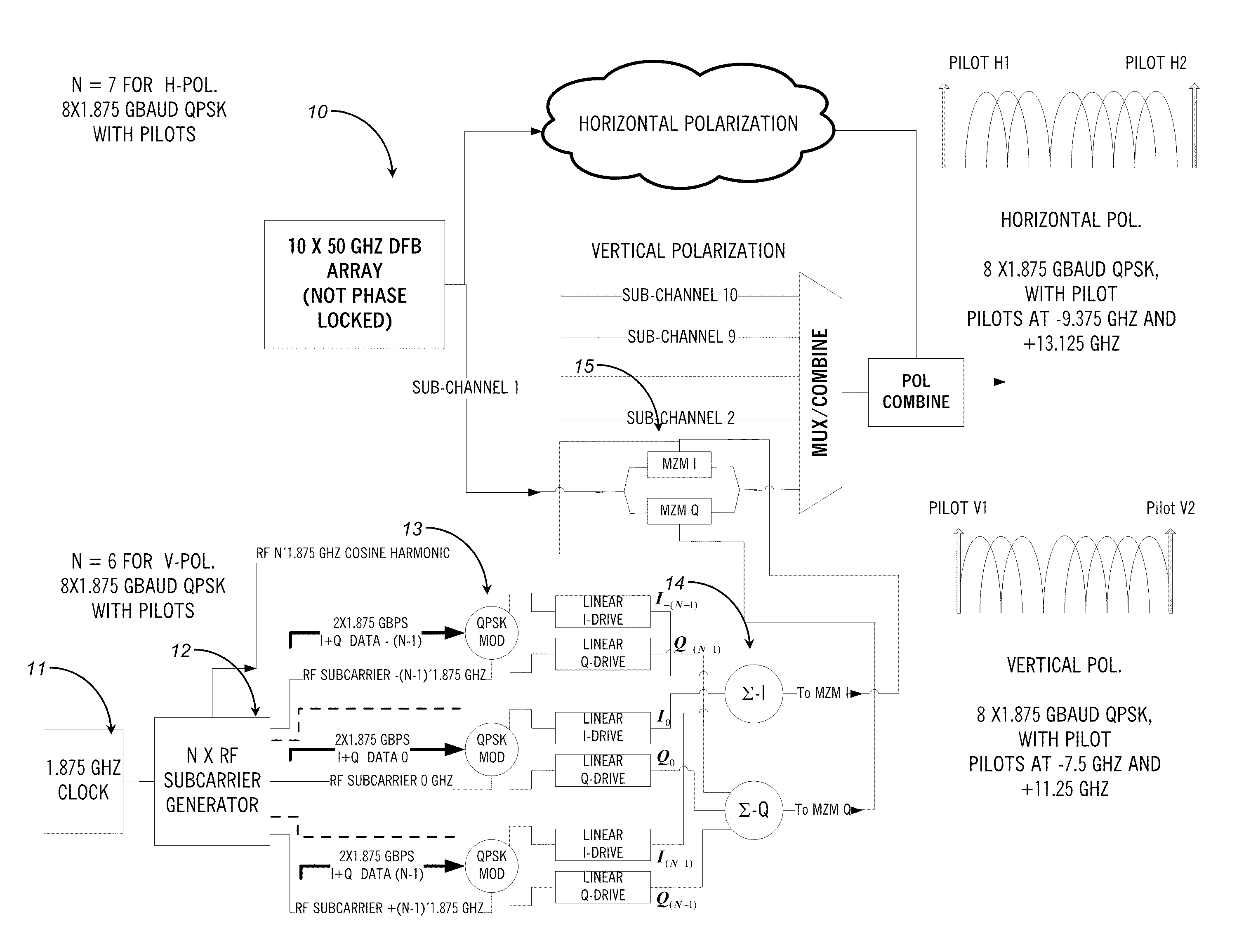
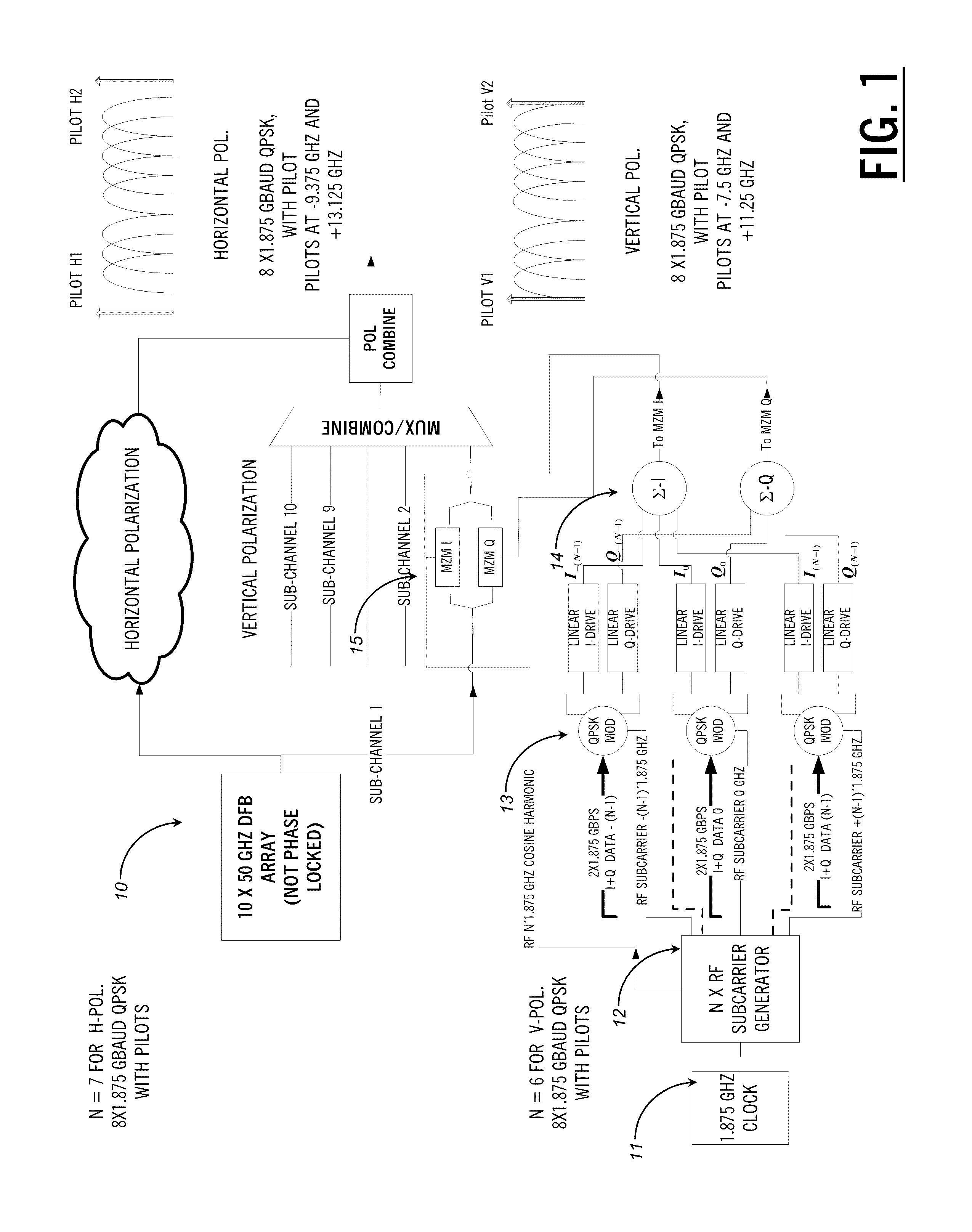
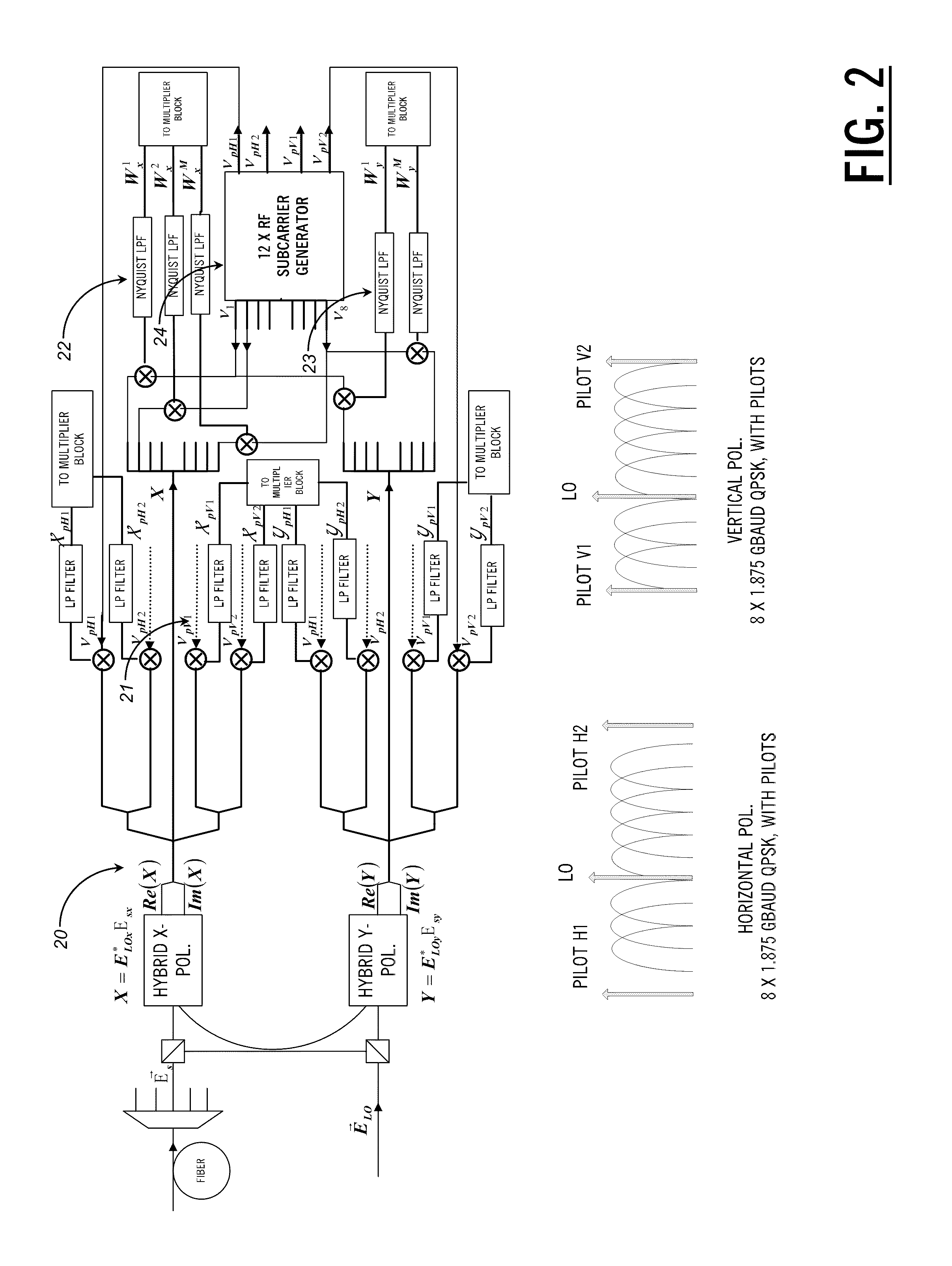
[0016]In various exemplary embodiments, the present disclosure provides an optical transceiver implementation that substantially simplifies the above DSP algorithms and, among other things: (1) may be scalable to XCVR designs carrying 1 Tbps and above, within a single circuit pack; (2) may partition capacity into low baud rate flows to simplify channel impairment compensation algorithms, thereby reducing circuit size and power consumption; (3) may be implementable in a highly integrated, preferably CMOS or BiCMOS, platform, that minimizes size, power consumption, and cost; (4) may allow spectral utilization efficiency to approach signal baud rate limits; (5) may allow the use of optical and electronic components, bandwidth limited to a fraction of the desired total capacity (i.e. ˜40 GHz in today's state of the art); (6) may provide sufficient tolerance to CD, PMD, and ASE noise to cover practical networks; (7) may be scalable to higher order modulation constellations, as desired; and (8) may use pilot tones and a combination of analog and digital signal processing to minimize optical and electronic complexity and power consumption.

Problems solved by technology

Unfortunately, this comes at a very substantial penalty of increased noise susceptibility, and, correspondingly, reduced optical unregenerated reach.
A further issue with current state of the art implementations is the high power consumption associated with the digital signal processing (DSP) algorithms that are used to modulate / demodulate the signals, and to compensate for a variety of communication channel impairments.
The drawbacks are substantial and include: low CD and PMD tolerance, an inability to scale to phase based or multi-bit / level symbol modulation formats, and poor ASE noise tolerance.
Disadvantages include the requirement for sophisticated DSP at the transmitter and receiver operating on the complete channel data, and a requirement for adding redundant cyclic prefix data.
A requirement for optoelectronic component bandwidth to cover a complete channel is detrimental.
Further, subcarriers within the OFDM channel are sufficiently low frequency such that complex phase recovery techniques are required.
Disadvantages are similar to coherent optical OFDM, dominated by signal processing complexity.
It is unlikely that such an approach is practical and realizable considering the associated electro-optic power consumption.
Further, sharp roll-off optical filters may be required in some implementations for sub-band separation.
Disadvantages stem from the fact that proper operation still requires optoelectronic bandwidth on the order of the total spectrum encompassing the complete channel, which is substantially beyond the state of the art, assuming a 1000 Gbps channel.
Some use lower bandwidth components, and, correspondingly, show a very substantial and detrimental performance penalty of several dB.
Non-orthogonal channel spacing still wastes a significant fraction of the overall spectrum.
The receiver for both approaches relies on DSP, which results in large chips with high power consumption, thereby substantially limiting the level of system integration that may be achieved.
A common theme to the problems outlined above is the high complexity of the electronic processing associated with providing the required detection and demodulation functions.
However, there are also significant problems with the DSP based approaches.
CMOS scaling problems that industry is currently encountering may be enumerated as follows: (1) scaling CMOS node geometry down does not appreciably help ADC power consumption and complexity, as one scales into deep submicron, and power is roughly fixed on a per Gsample per sec metric; (2) mask fabrication and circuit design tool costs are approximately doubling with every node generation; (3) cost per circuit function is staying roughly flat, i.e. cost per processed bit is ˜flat; (4) data rate increases are forced to ride the bleeding edge of CMOS processes; and (5) there is an energy per bit bottleneck, due to supply voltage Vdd saturation in deep submicron CMOS.

Method used


Image

  • Optical transceivers for use in fiber optic communication networks
  • Optical transceivers for use in fiber optic communication networks
  • Optical transceivers for use in fiber optic communication networks

Examples


Embodiment Construction

[0029]In various exemplary embodiments, the present disclosure provides an optical transceiver implementation that inherently simplifies the electronic signal processing design. This provides simplicity, an ability to use lower cost 65 nm CMOS geometries (i.e instead of 32 nm CMOS geometries, for example) or 130 nm BiCMOS geometries, for example, lowers overall power consumption, and provides a path to higher levels of power limited system density.

[0030]The individual building blocks used in the present disclosure, such as OFDM, pilot tones, etc., are generally known to those of ordinary skill in the art, in the broadest conceptual sense, however the present disclosure provides a unique feed forward algorithm for processing of the received signal, a unique combination of features and functionalities, and simplifications in the resulting signal processing algorithms that allow the introduction of analog signal processing in the high rate data path, while using digital algorithmic com...


PUM


Abstract

The present disclosure provides a polarization multiplexed transceiver, including: a transmitter; a receiver; circuitry within the transmitter configured to insert pilot tones as a reference state of polarization for a polarization multiplexed signal; and circuitry within the receiver configured to de-multiplex the polarization multiplexed signal using the pilot tones. The transmitted signal is constructed in such a manner as to facilitate the division of the receiver processing between the analog and digital domains such that the implementation may be simultaneously both highly spectrally efficient and power efficient.

Description

CROSS-REFERENCE TO RELATED APPLICATION[0001]The present disclosure is a continuation-in-part of co-pending U.S. patent application Ser. No. 12 / 691,474, filed on Jan. 21, 2010, and entitled “MULTI-CHANNEL OPTICAL TRANSCEIVER WITH OFFSET QUADRATURE AMPLITUDE MODULATION,” the contents of which are incorporated in full by reference herein.FIELD OF THE DISCLOSURE[0002]The present disclosure relates generally to optical transceivers for use in fiber optic communication networks. More specifically, the present disclosure relates to low power, coherent optical transceivers utilizing the self demultiplexed detection of polarization multiplexed signals.BACKGROUND OF THE DISCLOSURE[0003]Fiber optic communication networks are experiencing rapidly increasing capacity growth. This capacity growth is reflected by individual channel data rate scaling from 10 Gbps, to 40 Gbps, to currently developing 100 Gbps, to future projected 1000 Gbps channels. The capacity growth is also reflected by increasin...

Claims


Application Information

Patent Timeline
IPC IPC(8): H04J14/06
CPCH04B10/548H04B10/611H04B10/613H04B10/614H04L27/2697H04J14/0276H04J14/0298H04J14/06H04L5/0051H04B10/6166H04B10/65
Inventor GRIGORYAN, VLADIMIR S.FRANKEL, MICHAEL Y.WINGROVE, MICHAEL J.
Owner CIENA
Learn More