

High resistivity silicon wafer produced by a controlled pull rate czochralski method
a high-resistivity, silicon wafer technology, applied in the direction of polycrystalline material growth, crystal growth process, protective fluid, etc., can solve the problems of unfavorable decrease of limitation of the size of the resulting wafer, and very different final so as to prevent the resistivity of the wafer from diminishing, reduce the density and size of ingrown defects, and high resistivity
- Summary
- Abstract
- Description
- Claims
- Application Information
AI Technical Summary
Benefits of technology
Problems solved by technology
Method used
Image

Examples
Embodiment Construction
The present invention now will be described more fully hereinafter with reference to the accompanying drawings, in which preferred embodiments of the invention are shown. This invention may, however, be embodied in many different forms and should not be construed as limited to the embodiments set forth herein; rather, these embodiments are provided so that this disclosure will be thorough and complete, and will fully convey the scope of the invention to those skilled in the art. Like numbers refer to like elements throughout.
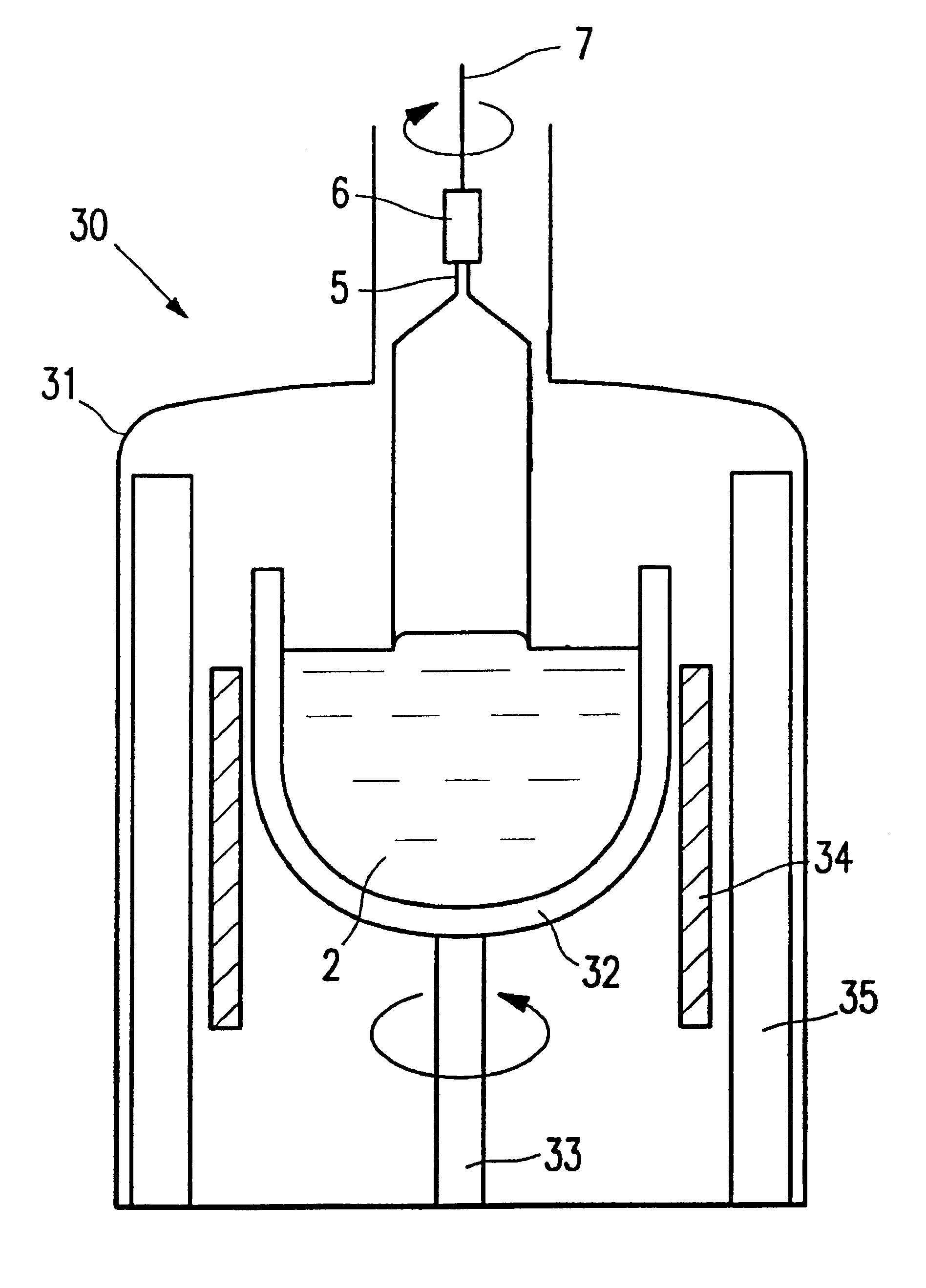
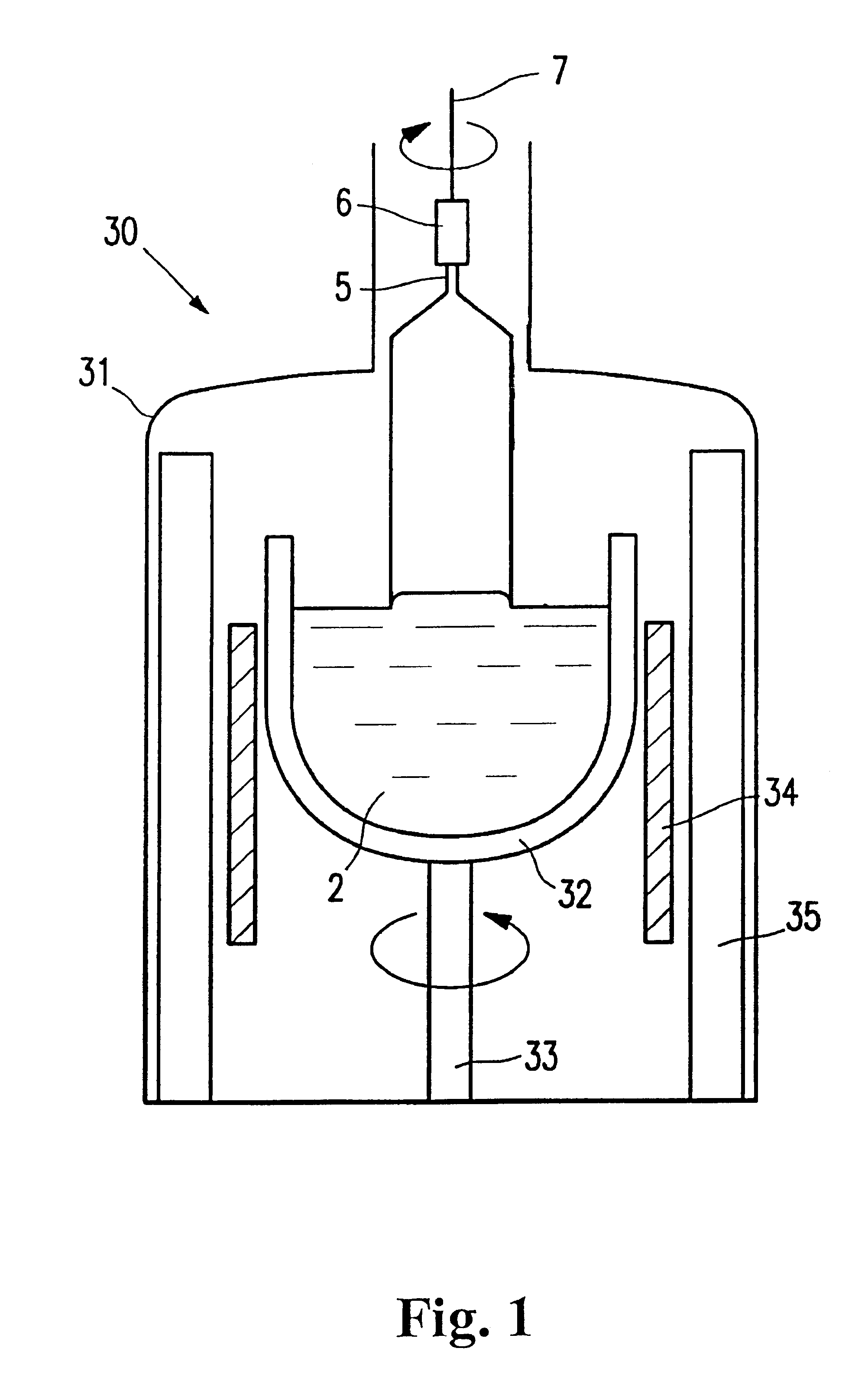
A method of obtaining a wafer exhibiting high resistivity and high gettering effect while preventing the reduction of resistivity due to the generation of oxygen thermal donors, and while further minimizing in-grown defects is provided by: a) using the CZ method to grow a silicon single crystal ingot having a resistivity of 100 .OMEGA..multidot.cm or more and an initial interstitial oxygen concentration of 10 to 40 ppma with a v / G ratio of from about 1.times.10....
PUM
| Property | Measurement | Unit |
|---|---|---|
| resistivity | aaaaa | aaaaa |
| resistivity | aaaaa | aaaaa |
| temperatures | aaaaa | aaaaa |
Abstract
Description
Claims
Application Information