Silicon single crystal pull-up apparatus and method of manufacturing silicon single crystal

a single crystal, pull-up technology, applied in the direction of crystal growth process, polycrystalline material growth, under a protective fluid, etc., can solve the problem of difficult to precisely measure the liquid surface level based on the mirror image of the reference reflector reflected on the liquid surface, and achieve the effect of convenient connection, improved resistivity distribution, and convenient setting of purging tubes

Active Publication Date: 2011-10-27
SUMCO CORP
View PDF4 Cites 22 Cited by
  • Summary
  • Abstract
  • Description
  • Claims
  • Application Information

AI Technical Summary

Benefits of technology

[0018]In the present invention, it is preferable that the camera photographs the mirror image in a state where the purging tube does not exist on the optical axis, and the conversion table creator creates the conversion table representing a relationship between the liquid surface level obtained when the liquid surface level of the silicon melt is arbitrarily changed while lifting and lowering the crucible before start of a single crystal pull-up process and the position of the mirror image in the state where the purging tube does not exist. With this configuration, the influence of the purging tube can be grasped more precisely, thereby reliably eliminating the influence of the purging tube included in measurement results of the liquid surface level.
[0019]In the present invention, it is preferable that the thermal radiation shield have a shield main body having a reverse conical trapezoidal shape whose diameter is increased from its lower end toward its upper end and an inside flange portion formed so as to horizontally extend from the lower end portion of the shield main body toward the inside and that the purging tube be placed on the upper surface of the inside flange portion. With this configuration, it is possible to easily set the purging tube, facilitating connection between the thermal radiation shield and the purging tube.
[0020]As described above, according to the present invention, it is possible to precisely measure the liquid surface level even in the case where the purging tube is provided inside the thermal radiation shield to improve stability in the distribution of resistivity of the silicon single crystal in the pull-up direction.

Problems solved by technology

However, in conventional silicon single crystal pull-up apparatus using the purging tube, the purging tube has a cylindrical shape, so that the image of the liquid surface captured through the purging tube is also distorted depending on the installation position, thickness, surface condition and the like of the purging tube, which makes it very difficult to precisely measure the liquid surface level based on the mirror image of the reference reflector reflected on the liquid surface.

Method used


Image

  • Silicon single crystal pull-up apparatus and method of manufacturing silicon single crystal
  • Silicon single crystal pull-up apparatus and method of manufacturing silicon single crystal
  • Silicon single crystal pull-up apparatus and method of manufacturing silicon single crystal

Examples


first embodiment

[0058]FIG. 5 is a flowchart illustrating a silicon single crystal manufacturing method according to the

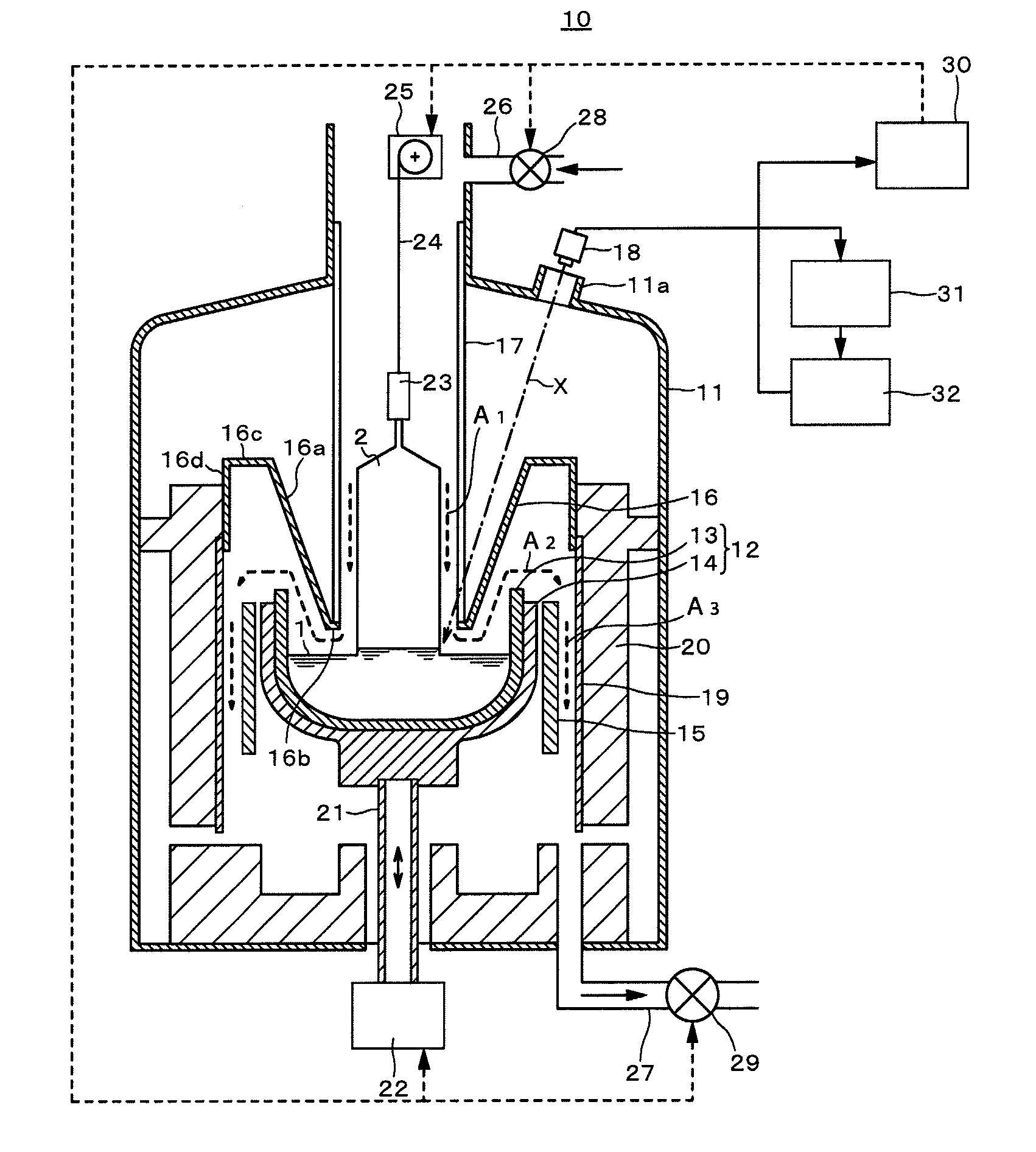
[0059]As shown in FIG. 5, in the manufacturing process of the silicon single crystal according to the first embodiment, an appropriate amount of polycrystalline silicon nuggets are packed into the crucible 12. Then, after the inside of the chamber 11 is set under an Ar gas atmosphere at a reduced pressure, the crucible is heated by the heater 15 to melt the silicon raw material in the crucible (S101). At this time, the seed crystal provided at the distal end of the wire 24 is located to be sufficiently higher than the quartz crucible and is spaced apart from the polysilicon which is being melted.

[0060]Next, after temperature control of the silicon melt 1 is performed until the silicon melt 1 is stabilized, the height of the crucible 12 is adjusted to set an initial liquid surface level h0 of the silicon melt (S102). Although not especially limited, the setting of the initial liquid...

second embodiment

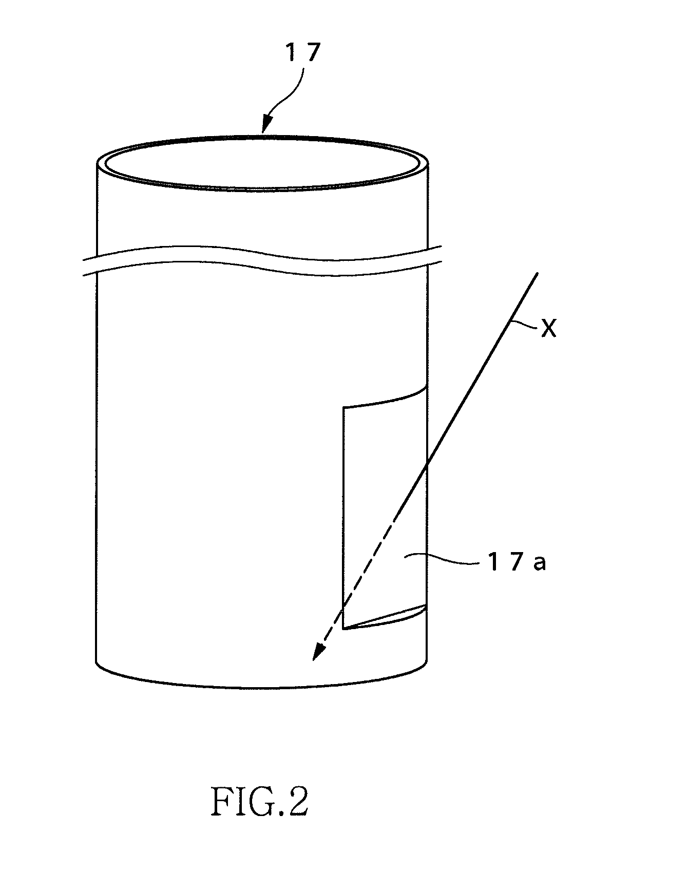
[0074]FIG. 7 is a flowchart illustrating a silicon single crystal manufacturing method according to the FIGS. 8A and 8B are cross-sectional views each schematically illustrating a state of the purging tube 17. FIG. 8A illustrates a state where the purging tube 17 has been pulled up, and FIG. 8B illustrates a state where the purging tube 17 is in a normal position.

[0075]As shown in FIG. 7, in the manufacturing process of the silicon single crystal according to the second embodiment, the polycrystalline silicon nuggets in the crucible 12 are heated by the heater 15 to be melted (S201), as in the first embodiment.

[0076]Next, after temperature control of the silicon melt 1 is performed until the silicon melt 1 is stabilized, the height of the crucible 12 is adjusted to set an initial liquid surface level h0 of the silicon melt (S202). Although not especially limited, the setting of the initial liquid surface level h0 can be achieved by an operator raising and lowering the crucible whil...


PUM

PropertyMeasurementUnit
diameteraaaaaaaaaa
cylindrical shapeaaaaaaaaaa
liquid surface level calculatoraaaaaaaaaa

Abstract

A silicon single crystal pull-up apparatus is provided with a chamber into which an inert gas is introduced; a crucible that supports a silicon melt within the chamber; a heater that heats the silicon melt in the crucible; a lifting device for lifting and lowering the crucible; a thermal radiation shield disposed above the crucible; a cylindrical purging tube that is provided inside the thermal radiation shield so as to straighten the inert gas; a CCD camera that photographs the mirror image of the thermal radiation shield reflected on the liquid surface of the silicon melt through the purging tube; a liquid surface level calculator that calculates the liquid surface level of the silicon melt from the position of the mirror image photographed by the camera; and a conversion table creator that creates a conversion table representing a relationship between the liquid surface level of the silicon melt and the mirror image position obtained. The liquid surface level calculator calculates the liquid surface level based on the conversion table.

Description

BACKGROUND OF THE INVENTION[0001]1. Field of the Invention[0002]The present invention relates to a silicon single crystal pull-up apparatus and a method of manufacturing a silicon single crystal and, more particularly, to a method of measuring and controlling a liquid surface level of silicon melt.[0003]2. Description of Related Art[0004]As a typical manufacturing method of a silicon single crystal for semiconductor devices, a Czochralski Method (CZ method) is known. In the CZ method, polycrystalline silicon nuggets are packed into a quartz crucible and heated by a heater for melting. Then, a seed crystal dipped into the obtained silicon melt is rotated with respect to the crucible while gradually pulling up the seed crystal to grow a silicon single crystal.[0005]There may be a case where an impurity (dopant) such as arsenic (As) or antimony (Sb) is doped in a silicon melt for the purpose of adjusting the resistivity of the silicon single crystal in accordance with characteristics o...

Claims


Application Information

Patent Timeline
Patent Type & Authority Applications(United States)
IPC IPC(8): C30B15/20
CPCC30B15/20C30B15/26Y10T117/1068C30B35/00C30B29/06
Inventor TAKANASHI, KEIICHIHAYASHI, KENGONARUSHIMA, YASUHITO
Owner SUMCO CORP
Why Eureka
Try Eureka