All-digital frequency synthesis with dco gain calculation

a digital frequency and gain calculation technology, applied in the field of communication, can solve the problems of difficult integration of analog baseband with digital baseband, low dco gain, and low dco gain,

Inactive Publication Date: 2011-10-27
TEXAS INSTR INC
View PDF4 Cites 15 Cited by
  • Summary
  • Abstract
  • Description
  • Claims
  • Application Information

AI Technical Summary

Problems solved by technology

Analog and RF circuits, on the other hand, do not scale down very well.
More difficult would be integrating the analog baseband with the digital baseband.
In addition, the low amount of voltage headroom challenges one to find new circuit and architecture solutions.
Integrating the analog baseband into the RF transceiver section presents a different set of challenges: The conventional Bi-CMOS RF process is tuned for high-speed operation with a number of available passive components and does not fundamentally stress high precision.
In a deep-submicron CMOS design, the silicon area is often bond-pad limited.
Deep-submicron CMOS processes present new integration opportunities on one hand, but make it extremely difficult to implement traditional analog circuits, on the other.
For example, frequency tuning of a low-voltage deep-submicron CMOS oscillator is an extremely challenging task due to its highly nonlinear frequency vs. voltage characteristics and low voltage headroom making it susceptible to the power / ground supply and substrate noise.
In such low supply voltage case, not only the dynamic range of the signal suffers but also the noise floor rises, thus causing even more severe degradation of the signal-to-noise ratio.
Unfortunately, with each CMOS feature size reduction, the supply voltage needs also to be scaled down, which is inevitable in order to avoid breakdown and reliability issues.
Moreover, the high degree of integration leads to generation of substantial digital switching noise that is coupled through power supply network and substrate into noise sensitive analog circuits.
Furthermore, the advanced CMOS processes typically use low resistance P-substrate which is an effective means in combating latchup problems, but exacerbates substrate noise coupling into the analog circuits.
This problem only gets worse with scaling down of the supply voltage.
RF synthesizers, specifically, remain one of the most challenging tasks in mobile RF systems because they must meet very stringent requirements of a low-cost, low-power and low-voltage monolithic implementation while meeting the phase noise and switching transient specifications.
An important issue in digital VLSI and for intellectual property (IP)-based applications.

Method used


Image

  • All-digital frequency synthesis with dco gain calculation
  • All-digital frequency synthesis with dco gain calculation
  • All-digital frequency synthesis with dco gain calculation

Examples


Embodiment Construction

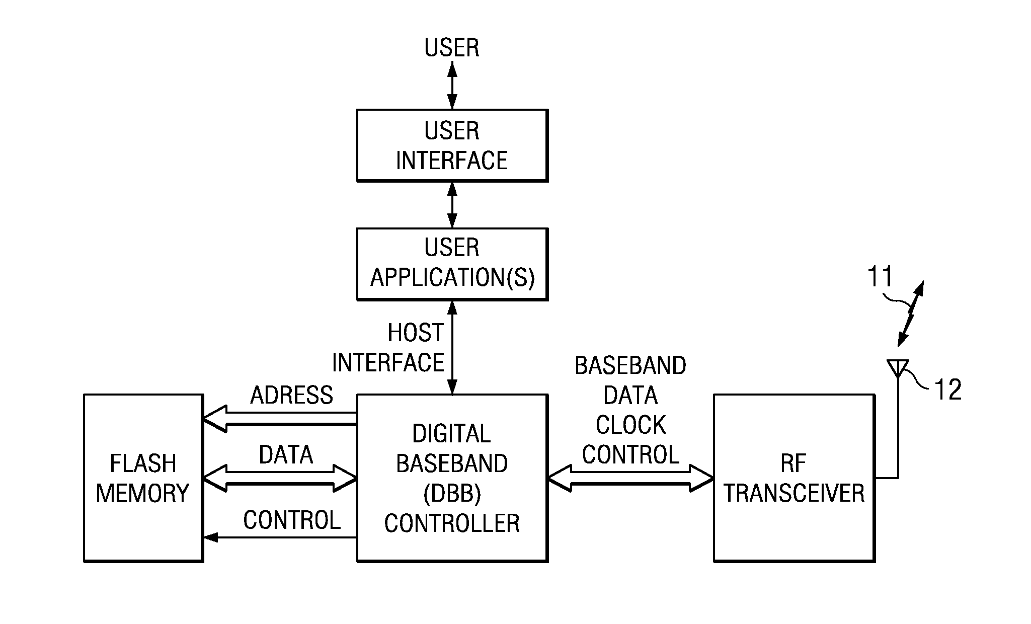
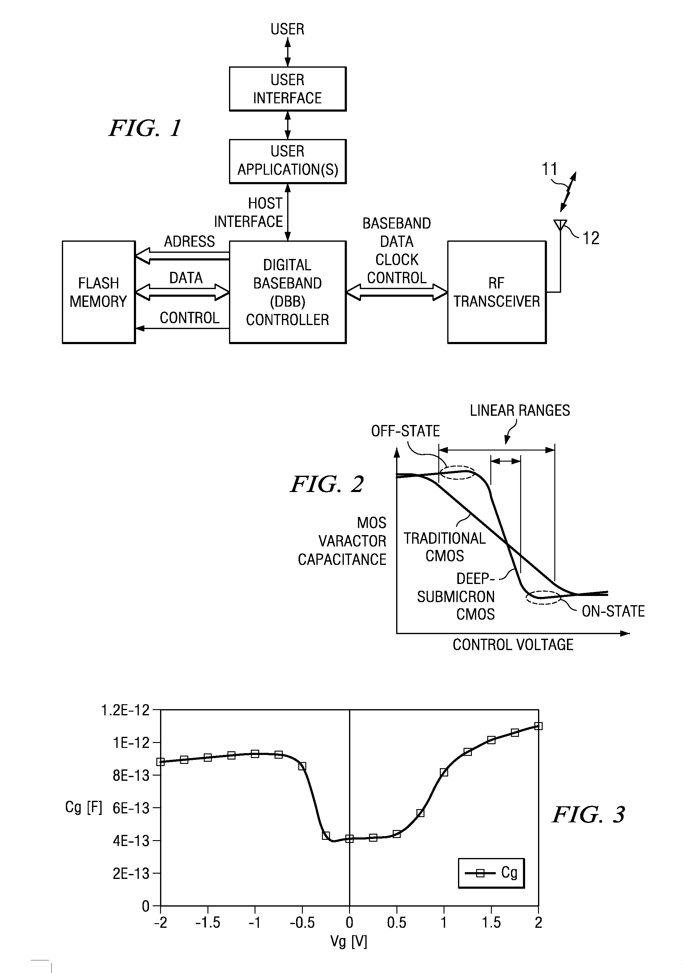
[0079]The ultimate goal in mobile wireless integration is a single-chip digital radio as shown in FIG. 1, although the present invention is not limited to use in a single chip digital radio design. In some examples, the digital baseband controller (DBB) can be based on a digital signal processor (DSP) or the ARM7 microprocessor and is responsible for taking the digital data stream from the RF transceiver and performing any necessary digital signal processing on it to convert the digital data stream into a stream of user data. Examples of the processing performed by the DBB controller may include digital filtering, data encoding and decoding, error detection and correction. It can also implement, for example, the GSM cellular or BLUETOOTH protocol layer stack which is controlled by a software program stored in a non-volatile flash memory. User applications running on, for example, a microprocessor or DSP, can communicate with the DBB controller and a user interface (e.g., a keypad, v...


PUM


Abstract

An all-digital frequency synthesizer architecture is built around a digitally controlled oscillator (DCO) that is tuned in response to a digital tuning word (OTW). In exemplary embodiments: (1) a gain characteristic (KDCO) of the digitally controlled oscillator can be determined by observing a digital control word before and after a known change (Δfmax) in the oscillating frequency; and (2) a portion (TUNE_TF) of the tuning word can be dithered (1202), and the resultant dithered portion (dkTF) can then be applied to a control input of switchable devices within the digitally controlled oscillator.

Description

[0001]This application claims the priority under 35 U.S.C. 119(e)(1) of the following copending U.S. provisional patent applications, all of which are incorporated herein by reference: 60 / 333,144 (Docket No. TI-33492) filed on Nov. 27, 2001; 60 / 333,115 (Docket No. TI-33500) filed on Nov. 27, 2001; 60 / 333,169 (Docket No. TI-33501) filed on Nov. 27, 2001; 60 / 343,846 (Docket No. TI-33500) filed on Dec. 28, 2001; 60 / 344,305 (Docket No. TI-33501) filed on Dec. 28, 2001; 60 / 343,837 (Docket No. TI-33492) filed on Dec. 28, 2001; and 60 / 386,290 (Docket No. TI-33501) filed on Jun. 5, 2002.FIELD OF THE INVENTION[0002]The invention relates generally to communications and, more particularly, to all-digital frequency synthesis for communications applications.BACKGROUND OF THE INVENTION[0003]A great reduction of the transistor feature size in recently developed deep-submicron CMOS processes shifts the design paradigm towards more digitally-intensive techniques. In a monolithic implementation, the ...

Claims


Application Information

Patent Timeline
Patent Type & Authority Applications(United States)
IPC IPC(8): H04B17/00H03L7/085H03L7/099
CPCH03L7/085H03L2207/50H03L7/0991
Inventor STASZEWSKI, ROBERT B.LEIPOLD, DIRKWALLBERG, JOHN
Owner TEXAS INSTR INC
Why Eureka
Try Eureka