Porous and non-porous nanostructures

a nanostructure and nanoporous technology, applied in the field of porous and non-porous nanostructures, can solve the problems of numerous limitations of current nanostructures relating to conductivity, resistance, porosity, and efficient fabrication methods

Active Publication Date: 2011-11-03
BOARD OF RGT THE UNIV OF TEXAS SYST
View PDF1 Cites 65 Cited by
  • Summary
  • Abstract
  • Description
  • Claims
  • Application Information

AI Technical Summary

Benefits of technology

[0011]A person of ordinary skill in the art will recognize that the porous structures and methods of the present invention can have numerous applications. For instance, the methods of the present invention can be utilized to fabricate nanowires, such as multi-layered silicon-based nanowires. Likewise, the structures of the present invention can have numerous applications, including applications as drug delivery vectors, drug delivery nanoneedles, bar-coded wires, and imaging agents.

Problems solved by technology

However, current nanostructures have numerous limitations relating to conductivity, resistance, porosity, and efficient fabrication methods.

Method used


Image

  • Porous and non-porous nanostructures
  • Porous and non-porous nanostructures
  • Porous and non-porous nanostructures

Examples


working example 1

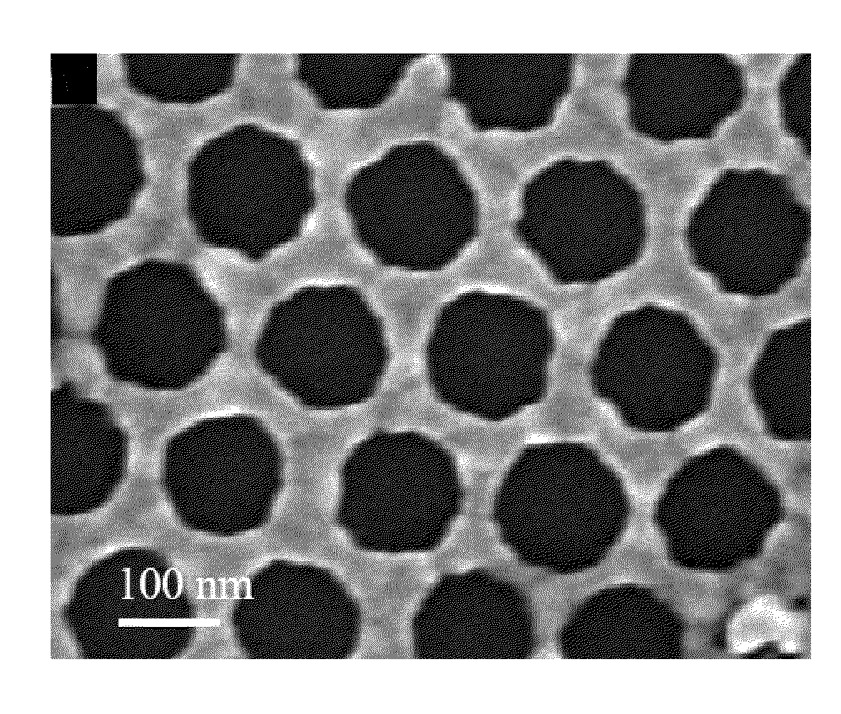
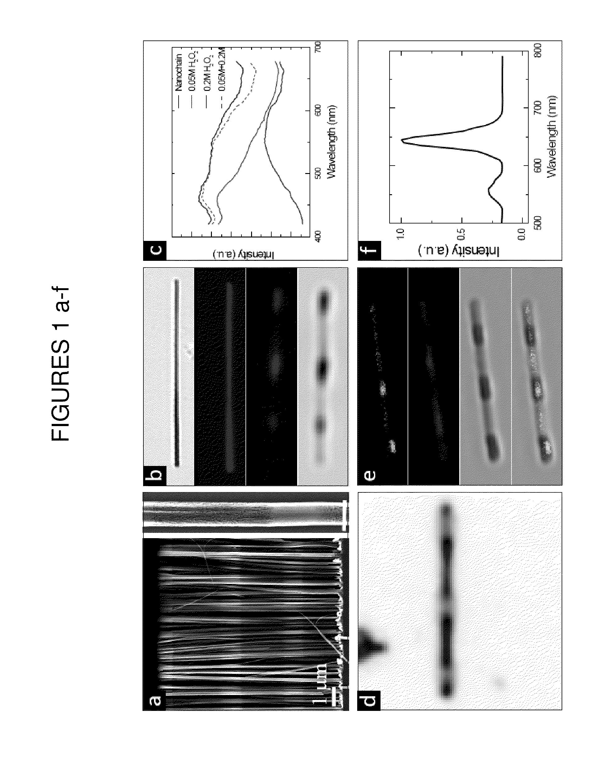
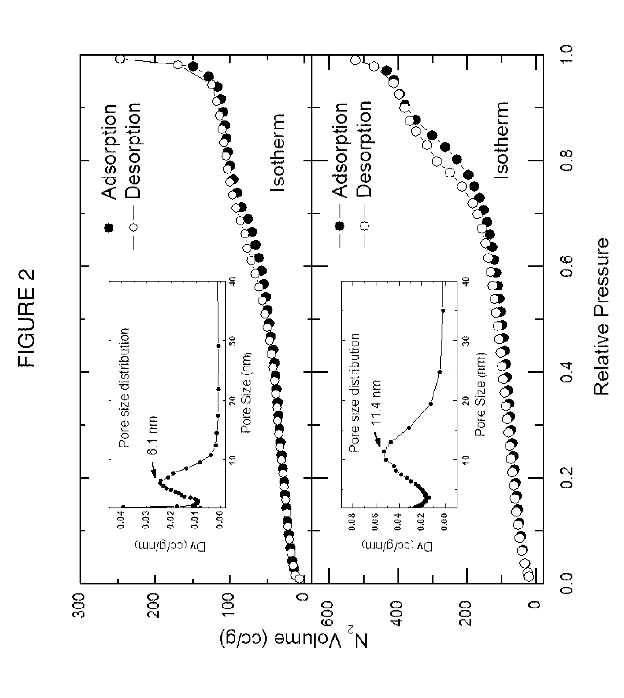
[0156]Silicon nanowires are intensively investigated in diverse fields such as energy production and storage, flexible electronics, and biomedicine due to the unique characteristics emerging from their one-dimensional semiconducting nature and their mechanical properties. Here, we show the synthesis of biodegradable porous silicon nanowires by metal assisted electroless etch of single crystal silicon with resistivity ranging from 0.0008 Ω-cm to 10 Ω-cm. Multicolor reflection and photoluminescence from a single porous silicon nanochain with periodically varying porosity was characterized. The geometry of porous nanowires was defined by nanolithography. Phase diagrams were developed to describe the synthesis of different nanostructures as a function of metal employed, H2O2 concentration, ethanol concentration and silicon resistivity. A mechanism has also been proposed to explain these observations. It was proven that porous silicon nanowires are biodegradable, and their life time can ...

working example 2

[0188]In this Example, porous silicon nanowires are fabricated by two step metal assisted electroless chemical etching of P-type or N-type silicon wafers. This method in combination with nanolithography or nanopatterning can be applied to fabricate porous silicon nanostructures of different shapes and sizes, such as nanorods, nanobelts, nanostrips, or nanochains. The specific resistivity of the silicon substrate and composition of the etching solution can determine the porosity and pore size (or lack thereof) of the resulting nanostructures. Silicon doping, type of metal catalyst, concentrations of H2O2, and solvent may all affect the formation of porous nanostructures at various resistivity ranges of silicon. A phase diagram summarizing the relation between porosification and doping, metal type, concentrations of H2O2, and solvent type can be generated.

Introduction

[0189]Metal ion assisted electroless etching of silicon nanowires has attracted a lot of attention as a facile, reliabl...


PUM

PropertyMeasurementUnit
aspect ratioaaaaaaaaaa

Abstract

Disclosed are a variety of porous and non-porous wire-like structures of microscopic and nanoscopic scale. For instance, disclosed are structures that comprise a porous object that comprises: (i) a first region; and (ii) a second region adjacent to the first region along an axis of the object, where the first region has at least one porous property different from that of the second region. Also disclosed are structures that include: (i) a high resistivity silicon; and (ii) a cross-section that is substantially perpendicular to an axis of the object. Also disclosed are methods of making and using such structures. For instance, the present invention provides methods of making a porous object by: (i) obtaining an etchable substrate; (ii) forming on a surface of the substrate a patterned porosification assisting metal layer that has at least one opening; and (iii) subsequently exposing the substrate to a first etching solution and a second etching solution to form respectively a first region and a second region of a porous object.

Description

CROSS REFERENCE TO RELATED APPLICATION[0001]This application claims priority to U.S. Provisional Patent Application No. 61 / 282,627 filed on Mar. 9, 2010, the entirety of which is incorporated herein by reference.STATEMENT REGARDING FEDERALLY SPONSORED RESEARCH[0002]This invention was made with government support under Grant No. NNJO6HEO6A, awarded by the National Aeronautics and Space Administration; Grant Nos. CA128797 and CA122864, both awarded by the National Institutes of Health; Grant No. W911NF-09-1-0044, awarded by the Defense Advanced Research Projects Agency; and Grant Nos. W81XWH-07-2-0101 and W81XWH-09-1-0212, both awarded by the U.S. Department of Defense. The government has certain rights in the invention.BACKGROUND OF THE INVENTION[0003]Porous and non-porous nanostructures, such as silicon-based nanostructures, have many applications in many fields, including applications in electro-optical devices, sensors, solar cells, nanowires, and drug delivery. However, current n...

Claims


Application Information

Patent Timeline
Patent Type & Authority Applications(United States)
IPC IPC(8): H01L29/06H01L21/306B82Y40/00B82Y99/00
CPCB82Y30/00Y10T428/2982H01L29/0665B82Y10/00B82Y40/00H01L2924/0002H01L2924/00
Inventor FERRARI, MAUROLIU, XUEWUCHIAPPINI, CIROFAKHOURY, JEAN RAYMOND
Owner BOARD OF RGT THE UNIV OF TEXAS SYST
Why Eureka
Try Eureka