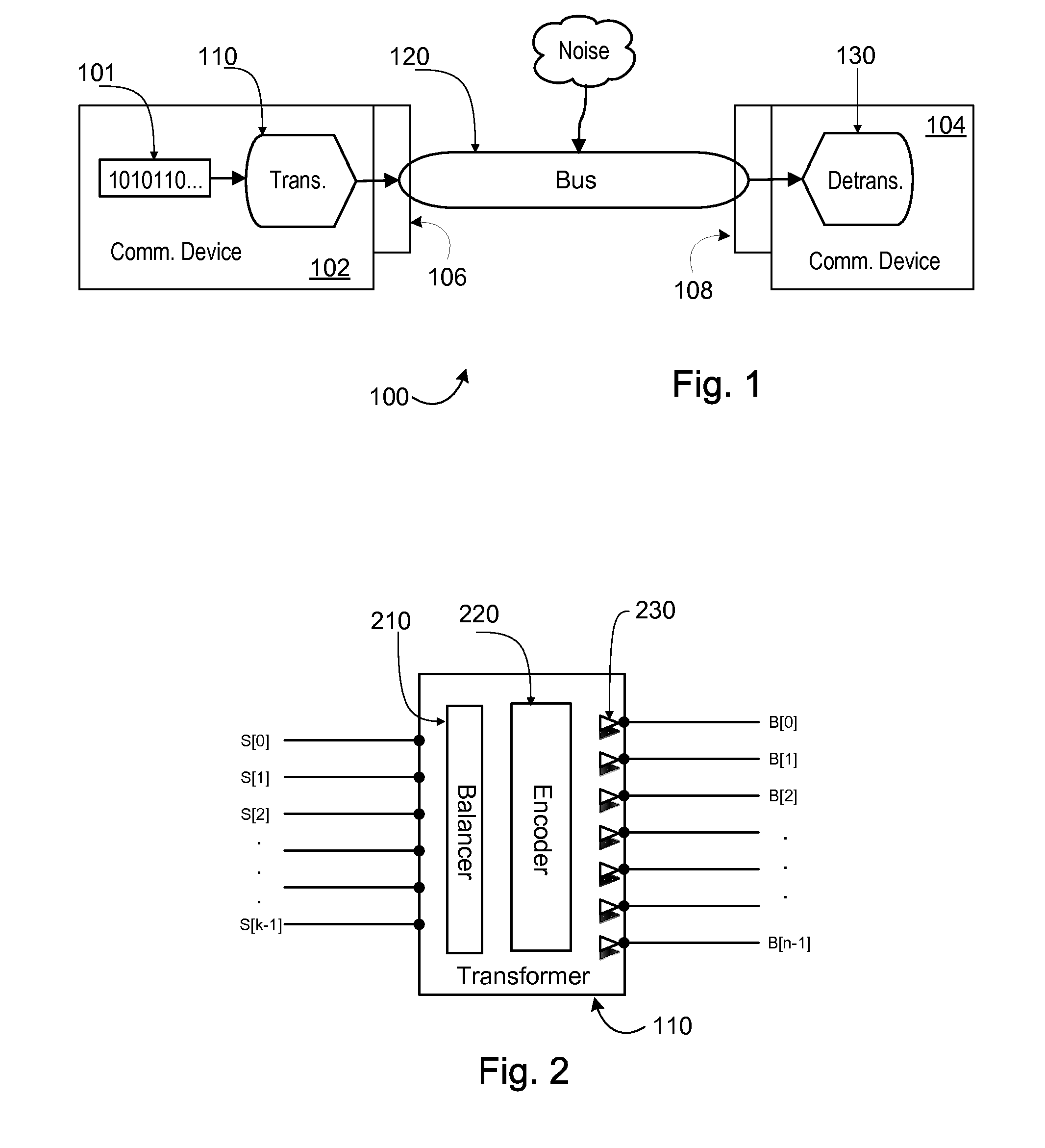
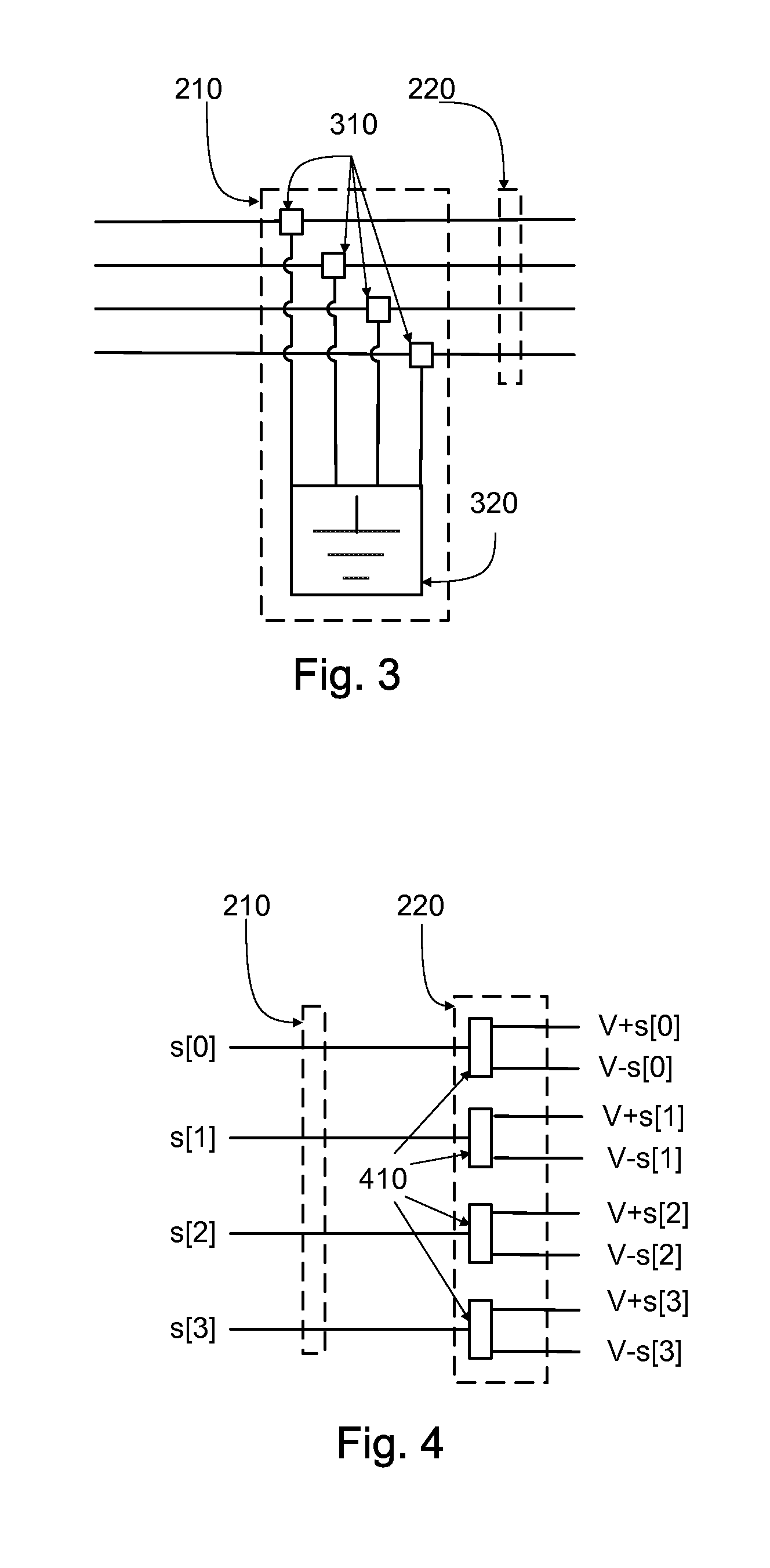
[0043]FIG. 3 depicts aspects of example components facilitating single-ended signaling. Units 310 may be understood as performing a balancing function corresponding to the balancer 210 (FIG. 2). These units 310 create for every incoming signal another signal that can differ with respect to the reference 320. Where these signals correspond to voltages, these units put on their outgoing wires one of two possible voltages wherein these voltages depend on the reference 320. For example, these units could put a
voltage of V or V+a on these wires where V is the
voltage of the reference point and a is a predetermined
voltage. These voltages are then forwarded directly to the
bus 120, so that no components corresponding to the
encoder 220 are necessary in this case. The pin-efficiency of single-ended signaling is 1.0 or 100%. However, single-ended signaling suffers from a plurality of noise types, as described earlier. A common approach to alleviate these problems is to increase the value of a thereby increasing the
total energy consumption. However, in applications this may lead to other disadvantageous effects (such as battery drain, or induction of noise on other devices).
[0044]FIG. 4 depicts aspects of example components facilitating conventional
differential signaling. In this example, the input signals are designated s[0], . . . , s[3]. No components corresponding to the balancer 210 (FIG. 2) are necessary in this example. Units 410 feeds two wires for each incoming signal s[0], . . . , s[3]. The amplitude of the signal put on the first wire is V+s[i] and that of the signal put on the second wire V−s[i] for i=0, 1, . . . , 3. The amplitude of the signals is chosen so that the difference in amplitude between the first and second wire is 2 s[i]. The value of V is typically unimportant, and can be chosen to be 0, since the information is encoded by the difference of the amplitudes of the signals put on the two wires. Units 410 may be understood as performing an encoding function corresponding to the
encoder 220.
[0045]
Differential signaling is resistant to some of the noise scenarios discussed above: it is resistant to
common mode noise since the information is encoded as the difference of voltages of two wires.
Differential signaling provides a better resistance to
bus noise than single-ended signaling. One of the reasons is that the swing in amplitude is twice as large as in single-ended signaling. As will be apparent to one of skill in the art, in single-ended signaling some transmission power may be wasted in a DC value of the transmitted signal.
Differential signaling does not introduce SSO noise in case of
chip-to-chip communication of NRZ-like signals. Finally, it is also resistant to
reference noise because no
external reference is required to reconstruct the original signals. However, differential signaling has that
disadvantage that its pin-efficiency is 0.5 or 50%.
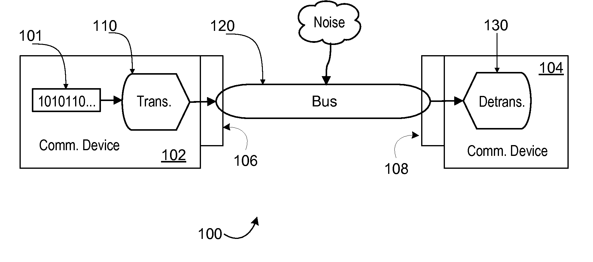
[0046]FIG. 5 depicts aspects of an example communication bus 500 in accordance with at least one embodiment of the invention. The communication bus 500 is an example of the bus 120 (FIG. 1). The bus 500 includes a plurality of signal paths such as the signal path 510. Each signal path may include transmission media such as wires (e.g., metallic wires) on which information is transmitted in the form of electrical voltages or currents. In chip-to-chip communications these wires may be on-chip interconnects, PCB traces or strip lines. Yet another application is DSL communications where each bus wire may correspond to one wire of a
twisted pair copper line typically used in DSL communications. A similar application is unshielded twisted pair (UTP)
Ethernet communications where again a wire of the bus 500 may correspond to one of the wires in a twisted pair. For communication between devices such as camera's, laptops, TVs, etc, the bus 500 may be in accordance with any suitable conventional communication standard and / or specification. In other embodiments, the signal paths can be optical cables transmitting optical signals in form of light. In yet other embodiments, the signal paths can be media suited to the transmission of signals.
[0047]In at least one embodiment of the invention, each signal is physical, tangible and / or non-transitory in time. In at least one embodiment of the invention, a physical signal is a signal that is tangibly embodied in a tangible and / or physical transmission media. In at least one embodiment of the invention, transformation of signals includes physical transformation of physical signals as part of a physical mechanism. In at least one embodiment of the invention, signals are tangible aspects of an apparatus. In at least one embodiment of the invention, signals are transformed by a mechanism in accordance with physical principles well known to those of skill in the art.Example of Orthogonal Differential Vector Signaling
[0048]The description now turns to an example of orthogonal differential vector signaling with reference to FIG. 6. FIG. 6 depicts aspects of an example
transformer 600 in accordance with at least one embodiment of the invention. The
transformer 600 has a pin-efficiency of 0.75 or 75%, and has input including three signals b[0], b[1] and b[2]. These signals represent the information in the
information storage medium 101. The balancer 210 creates four signals s[0], s[1], s[2] and s[3] from the incoming three signals b[0], b[1] and b[2]. The first signal s[0] is set to V and the other signals s[1], s[2] and s[3] are set with respect to this first signal s[0]. This task is done by the units 610 which set s[i] to b[i−1]−V for i=1, 2, 3. Depending on the application V can be set to 0 or some other suitable value. In chip-to-chip communication b[0], b[1] and b[2] may be single-ended NRZ signals with associated signal levels of a and 0. In this case V may be set to a / 2 to remove the mean value of the single-ended NRZ signal. The four generated signals s[0], s[1], s[2] and s[3] may then enter the
encoder 220. The encoder 220 may include various components such as adders such as
adder 630, subtractors such as
subtractor 631, multipliers such as multiplier 640, and paths connecting these components such as paths 621, 622, 623, 635 and 636. In at least one embodiment, the multipliers are incorporated into the drivers 230. A task of the adders is to add incoming values and pass them on the outgoing paths. A task of the subtractors is to subtract the lower incoming value from the upper one and pass it on the outgoing paths. A task of the multipliers is to multiply the incoming value by a suitable factor (e.g., 0.5 in this case) and to pass it along the outgoing path. For example, the
adder 630 computes the addition of the values of its incoming paths 635 and 622 which is s[0]+s[1] and passes it on the paths 635 and 636. Similarly, the
subtractor 631 subtracts the value of its lower incoming path 621, namely s[1], from the value of its upper incoming path, namely s[0], and passes on the result s[0]−s[1] along its outgoing paths. The output of the encoder 220 is four values W[1], . . . , W[4].

