Method for producing an electric functional layer on a surface of a substrate

Inactive Publication Date: 2011-11-10
SIEMENS AG
View PDF4 Cites 6 Cited by
  • Summary
  • Abstract
  • Description
  • Claims
  • Application Information

AI Technical Summary

Benefits of technology

[0010]The proposed has the advantage that an electrical connection can be produced cost-effectively and quickly by planar technology. The electronic module produced by the method only has a low installation height. Compared with thermal flame spraying, highly dense layers can be produced. The functional layer exhibits high electrical as well as high thermal conductivity. The functional layer is wear resistant and very hard, even though only a low heat input into the substrate takes place during production. As very high application rates exceeding 100 μm per minute are possible the process times for the manufacture of electric functional layers can be reduced to minutes.
[0014]According to one embodiment, the electric functional layer is applied to the entire surface of the substrate. This makes it possible to produce all-over or only partial shields to improve EMC behavior.
[0016]To locally improve heat removal, provision can also be made during the manufacture of the electric functional layer for producing sections of different thickness. The thicker the conductive layer, the better the heat removal.
[0020]Expediently, a sacrificial layer is applied to the surface of the substrate before application of the electric functional layer. The sacrificial layer prevents the components on the substrate from being damaged by the particles impacting at high kinetic energy.

Problems solved by technology

Owing to the numerous steps required, however, this connection technology entails higher costs.
The material used for the mask can be a polymer for example which results in poor adhesion of the particles on the mask.

Method used


Image

  • Method for producing an electric functional layer on a surface of a substrate
  • Method for producing an electric functional layer on a surface of a substrate

Examples


Embodiment Construction

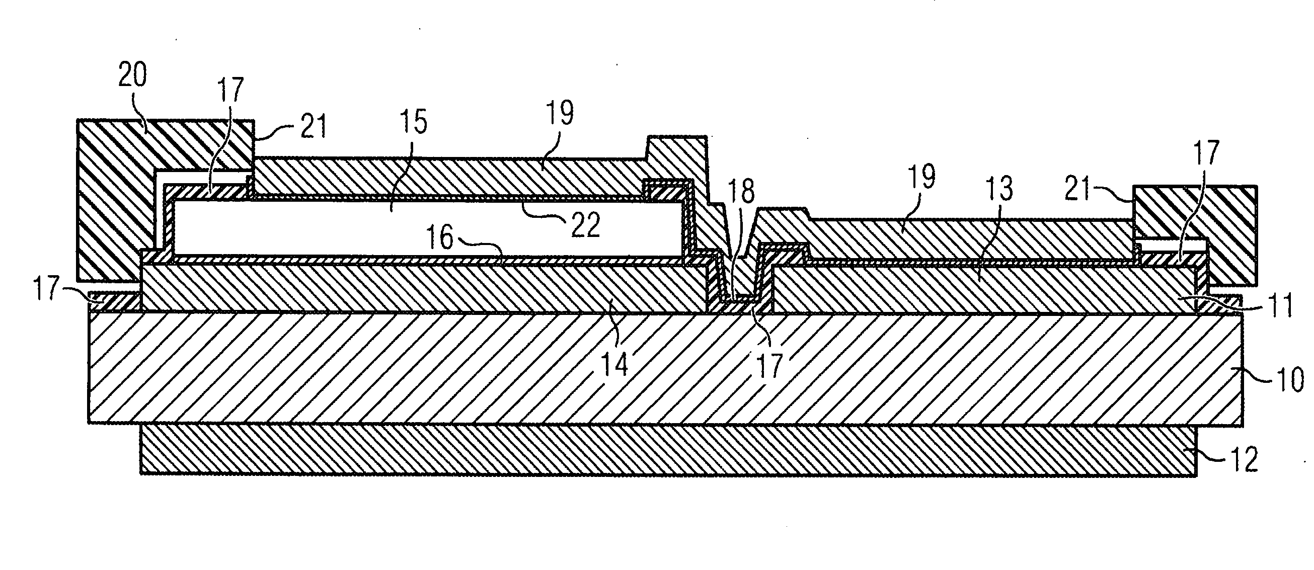
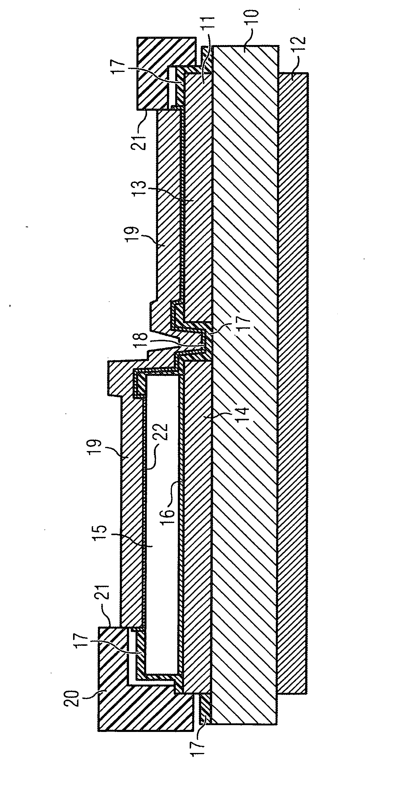
[0027]Reference will now be made in detail to the preferred embodiments of the present invention, examples of which are illustrated in the accompanying drawing, wherein like reference numerals refer to like elements throughout.

[0028]A metal layer 11, for example made of copper, is formed on a top side of a substrate 10. The substrate 10 can for example be made of ceramic, printed circuit board material or flexible tape. The metal layer 11 exhibits a number of contact surfaces 13, 14, although only two contact surfaces are represented in the exemplary embodiment. On a bottom side opposite the top side of the substrate 10 a metal layer 12 is likewise formed, on which for example a heat sink can be arranged. For this purpose the metal layer 12 is, for example, formed over the entire surface and also made of copper.

[0029]For example a solder paste, a component 15, for example a power semiconductor component, is fixed to the contact surface 14 by an adhesive agent 16. The component exhib...


PUM

PropertyMeasurementUnit
Thicknessaaaaaaaaaa
Thicknessaaaaaaaaaa
Thicknessaaaaaaaaaa

Abstract

An electric functional layer is produced on a surface of a substrate, having at least an electronic component, particularly a semiconductor chip, provided thereof. The electric functional layer is formed using particles in powder of an electrically conductive material. The functional layer is blown on the surface of the substrate to form a thick and strong adhesive layer on impact with the substrate.

Description

CROSS REFERENCE TO RELATED APPLICATIONS[0001]This application is based on and hereby claims priority to German Application No. 10 2006 037 532.7 filed on Aug. 10, 2006 and PCT Application No. PCT / EP2007 / 057883 filed on Jul. 31, 2007, the contents of which are hereby incorporated by reference.BACKGROUND OF THE INVENTION[0002]The invention relates to a method for producing an electric functional layer on a surface of a substrate, on which at least one component, in particular a semiconductor chip, is arranged.[0003]The starting point for the production of an electronic module is a semi-finished product with a substrate to which a structured metal layer with metal or contact surfaces is applied. Some of the contact surfaces feature one or several components, for example a semiconductor chip or a passive component. The component or components is or are connected to the respective contact surface by an adhesive agent, usually solder. If one of the components exhibits a rear-side contact,...

Claims


Application Information

Patent Timeline
IPC IPC(8): H01L23/48H01L21/50
CPCH01L23/552H01L2924/014H01L24/80H01L24/82H01L2224/24011H01L2224/24051H01L2224/24226H01L2224/82039H01L2924/01015H01L2924/0102H01L2924/01029H01L2924/01033H01L2924/01047H01L2924/01082H01L2924/09701H01L2924/19041H01L2924/19043H01L2924/3025H05K3/102H05K3/14H05K3/32H05K2203/1344H05K2203/1469H01L2924/01005H01L2924/01006H01L2924/01023H01L2924/01075H01L24/24C23C24/04
Inventor HOLST, JENS-CHRISTIANJENSEN, JENS DAHLWEIDNER, KARLWEINKE, ROBERT
Owner SIEMENS AG
Why Eureka
Try Eureka