Solar cell and method for manufacturing the same

a solar cell and manufacturing method technology, applied in the field of solar cell and manufacturing the same, can solve the problems of increasing the recombination rate at the surface, affecting the conversion efficiency of the final product, and incurred a large amount of fabrication cost, so as to achieve the effect of improving the conversion efficiency

Inactive Publication Date: 2011-11-17
LG ELECTRONICS INC
View PDF2 Cites 4 Cited by
  • Summary
  • Abstract
  • Description
  • Claims
  • Application Information

AI Technical Summary

Benefits of technology

Because the first silicon thin film layer having such a configuration has a high film density, it has superior surface passivation characteristics to those of a silicon nitride film used as a passivation film in the related art. Thus, the first silicon thin film layer has improved step coverage characteristics. Also, because the first silicon thin film layer has a higher band gap (i.e., 1.8 eV) than that of crystalline silicon, it has an increased open circuit voltage, improving a conversion efficiency of the solar cell.
The emitter part may include a textured surface having fine protrusions and depressions. The emitter part may be configured such that a textured surface having a plurality of fine protrusions and depressions is formed at a front surface of the substrate by using dry etching, an emitter layer having a pre-set thickness is formed by spreading impurities at the front surface of the substrate, and at least a portion of the emitter layer having an impurity concentration that is higher than a solid solubility is removed by using dry etching. Thus, the emitter part, a portion of which has been removed by using dry etching, may have a thickness ranging from about 100 nm to 200 nm. Because the region having the impurity concentration higher than the solid solubility is removed from the emitter layer, a carrier mobility of the emitter part can be increased.
A first intrinsic semiconductor layer made of a-Si:H may be positioned between the emitter part and the first silicon thin film layer. In this instance, the first silicon thin film layer and the first intrinsic semiconductor layer may constitute a front passivation film, and the first intrinsic semiconductor layer improves passivation characteristics of the first silicon thin film layer.
The solar cell including the first and second silicon thin film layers may have a further increased band gap compared with a solar cell including only the first silicon thin film layer, so its open circuit voltage Voc can be maximized.
Because the region having the impurity concentration higher than the solid solubility is removed from the emitter layer, the mobility of carriers passing through the emitter part can be increased.
With these characteristics, the solar cell according to example embodiments of the present invention has effectively improved conversion efficiency.

Problems solved by technology

The monocrystalline silicon solar cell, having a high quality substrate, can easily accomplish as high an efficiency, but it is disadvantageous in that a great amount of fabrication cost is incurred.
In comparison, the polycrystalline silicon solar cell is disadvantageous in that it cannot accomplish high efficiency because its substrate is inferior to that of the mono-crystalline silicon solar cell, but recently, the substrate quality of the polycrystalline silicon solar cell has been improved and, as processing techniques of the polycrystalline silicon solar cell are advancing, the polycrystalline silicon solar cell is becoming highly efficient.
However, the solar cell having such a structure has a doubled surface area due to the protrusions and depression formed on the textured surface, so that a recombination rate at the surface increases.

Method used


Image

  • Solar cell and method for manufacturing the same
  • Solar cell and method for manufacturing the same
  • Solar cell and method for manufacturing the same

Examples


Embodiment Construction

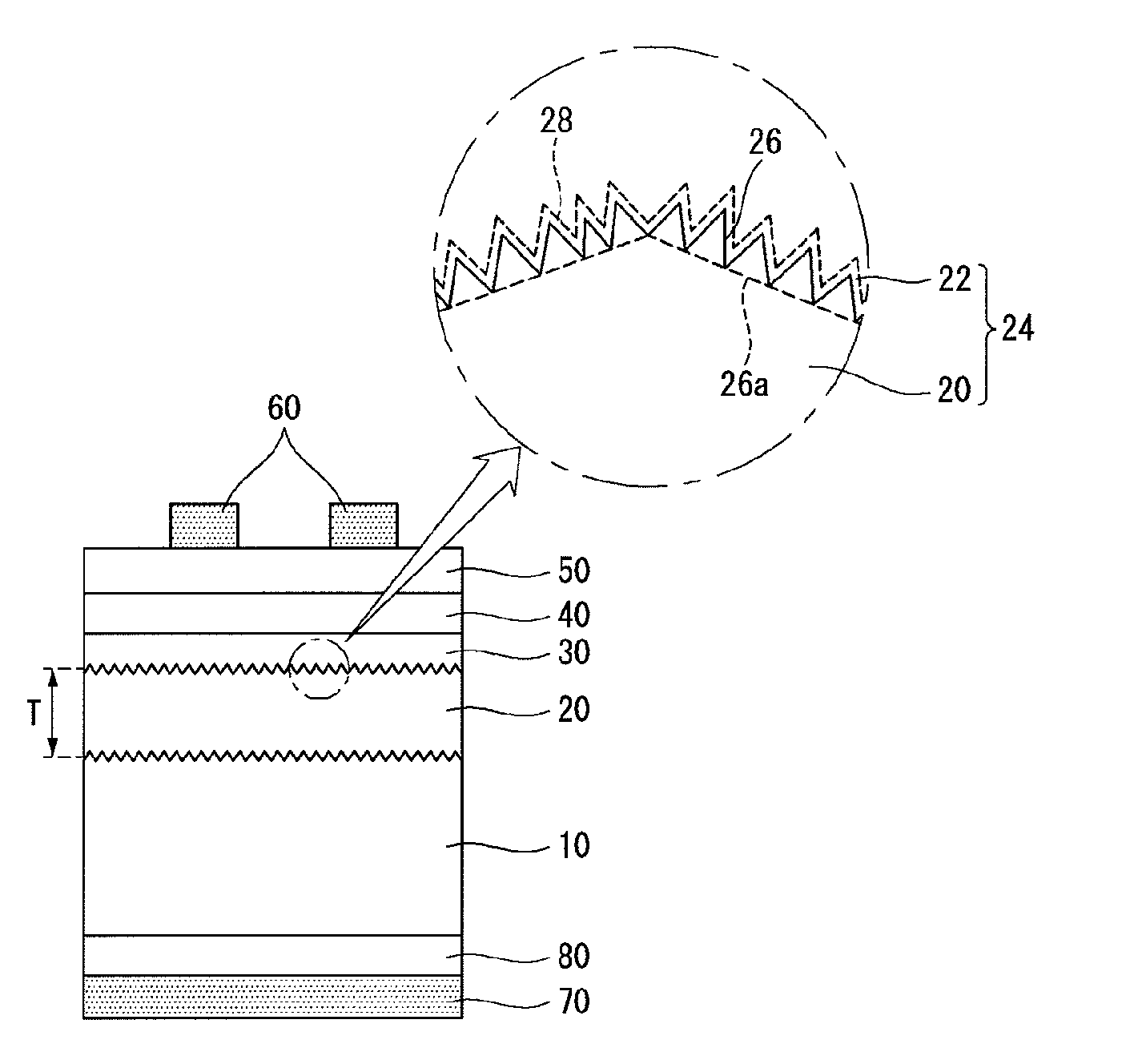
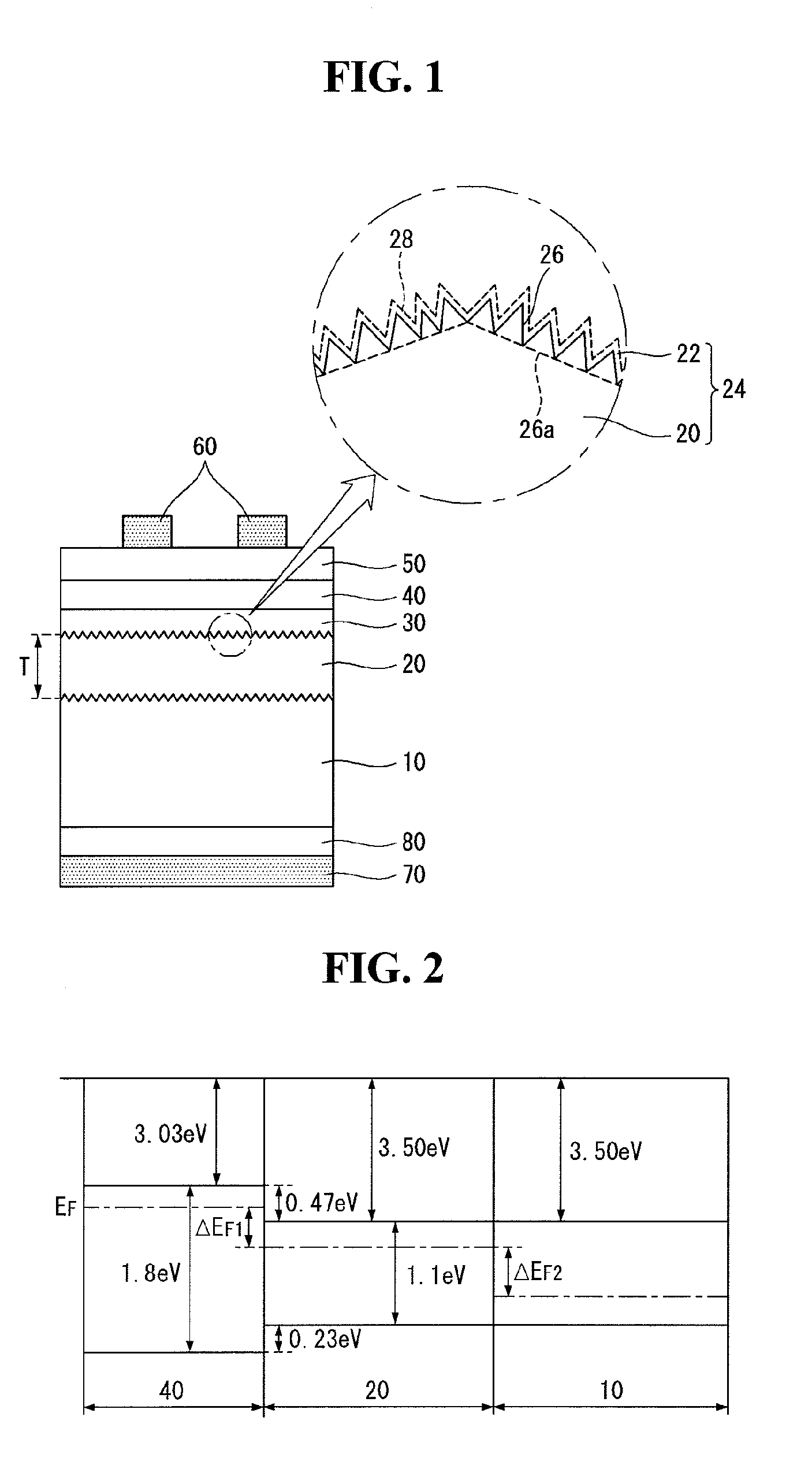
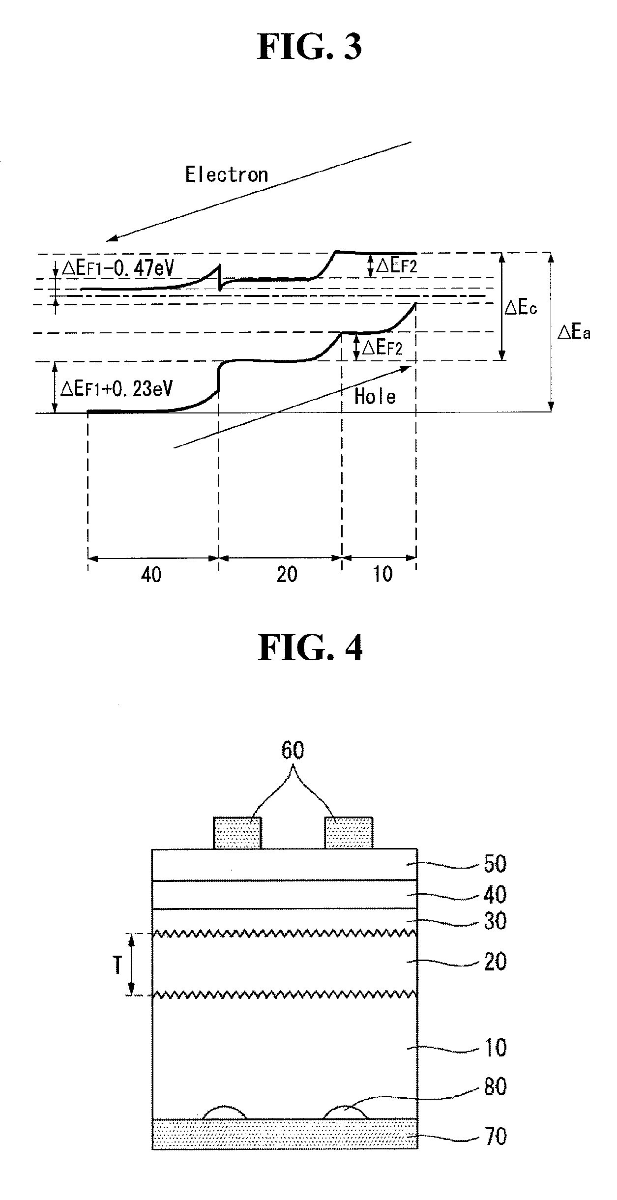
Example embodiments of the present invention will now be described in detail with reference to the accompanying drawings. The invention may, however, be embodied in many different forms and should not be construed as being limited to the embodiments set forth herein. Rather, these embodiments are provided so that this disclosure will be thorough and complete, and will fully convey the scope of the invention to those skilled in the art. In the drawings, the shapes and dimensions may be exaggerated for clarity, and the same reference numerals will be used throughout to designate the same or like components.

To clarify multiple layers and regions, the thicknesses of the layers are enlarged in the drawings. When it is said that any part, such as a layer, film, area, or plate, is positioned on another part, it refers to the part being directly on the other part or above the other part with at least one intermediate part. On the other hand, if any part is said to be positioned directly on ...


PUM


Abstract

A solar cell includes a substrate of a first conductive type; an emitter part of a second conductive type positioned at a front surface of the substrate; a first silicon thin film layer positioned on the emitter part and including amorphous silicon containing impurities of the second type that are doped therein; a first transparent conductive layer positioned on the first silicon thin film layer and electrically connected with the emitter part; a first electrode positioned on the first transparent conductive layer and electrically connected with the first transparent conductive layer; and a second electrode positioned on a back surface of the substrate. For example, the first silicon thin film layer includes N+-a-Si:H or N+-a-SiC:H.

Description

This nonprovisional application claims priority under 35 U.S.C. §119(a) to Patent Application No. 10-2010-0044128 filed in Republic of Korea on May 11, 2010, the entire contents of which are hereby incorporated by reference.BACKGROUND OF THE INVENTION1. Field of the InventionEmbodiments of the invention relate to a solar cell and method for manufacturing the same.2. Discussion of the Related ArtRecently, as exhaustion of existing energy resources such as oil or coal is foreseen, interest in alternative energy to replace them is increasing and a solar cell that produces electric energy from solar energy is receiving much attention.A solar cell is classified into a crystalline solar cell, an amorphous solar cell, a compound-based solar cell, and the like, depending on the kinds of materials used for the solar cell. Further, a crystalline silicon solar cell is classified into a mono-crystalline (or single crystalline) silicon solar cell and a polycrystalline silicon solar cell.The mono...

Claims


Application Information

Patent Timeline
Patent Type & Authority Applications(United States)
IPC IPC(8): H01L31/0236H01L31/18H01L31/0368
CPCH01L31/022425H01L31/02363H01L31/068Y02E10/547H01L31/1868Y02E10/52H01L31/1804Y02P70/50
Inventor LEE, KYOUNGSOOKIM, JONGHWANKANG, JUWANHA, MANHYOJANG, DAEHEE
Owner LG ELECTRONICS INC
Why Eureka
Try Eureka