Contact hole, semiconductor device and method for forming the same

Active Publication Date: 2011-11-17
INST OF MICROELECTRONICS CHINESE ACAD OF SCI
View PDF8 Cites 5 Cited by
  • Summary
  • Abstract
  • Description
  • Claims
  • Application Information

AI Technical Summary

Benefits of technology

[0045]In the method where a gate is formed first and then a contact hole is formed with a self-aligning process (i.e., forming a gate stack extending in a first direction, forming a gate from the gate stack and cutting the gate in a second direction different from the first direction, and then forming a contact hole with the self-aligning process), after the gate stack is cut, gaps are formed between gates, and contact holes are to be formed in the gaps. As the size of the gaps decreases, the possibility of interconnection between the contact holes increases. With an adjusted method for forming a gate, which comprises: forming a gate stack extending in a first direction, forming a contact hole with a self-aligning process, and then forming the gate from the gate stack and cutting the gate in a second direction different from the first direction; the contact hole is

Problems solved by technology

As the feature size of semiconductor devices is scaled, various microcosmic effects have been observed, resulting in more complex manufacturing processes of semiconductor devices, and difficulties in optimizing their performances.
Complex manufacturing processes require more masks and multistage photolithography, and it has become a challenging and pr

Method used


Image

  • Contact hole, semiconductor device and method for forming the same
  • Contact hole, semiconductor device and method for forming the same
  • Contact hole, semiconductor device and method for forming the same

Examples


first embodiment

[0056]According to the invention, a method for forming a contact hole comprises the following steps.

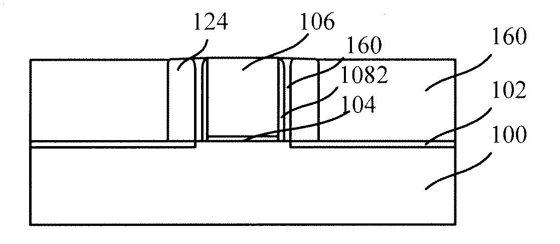
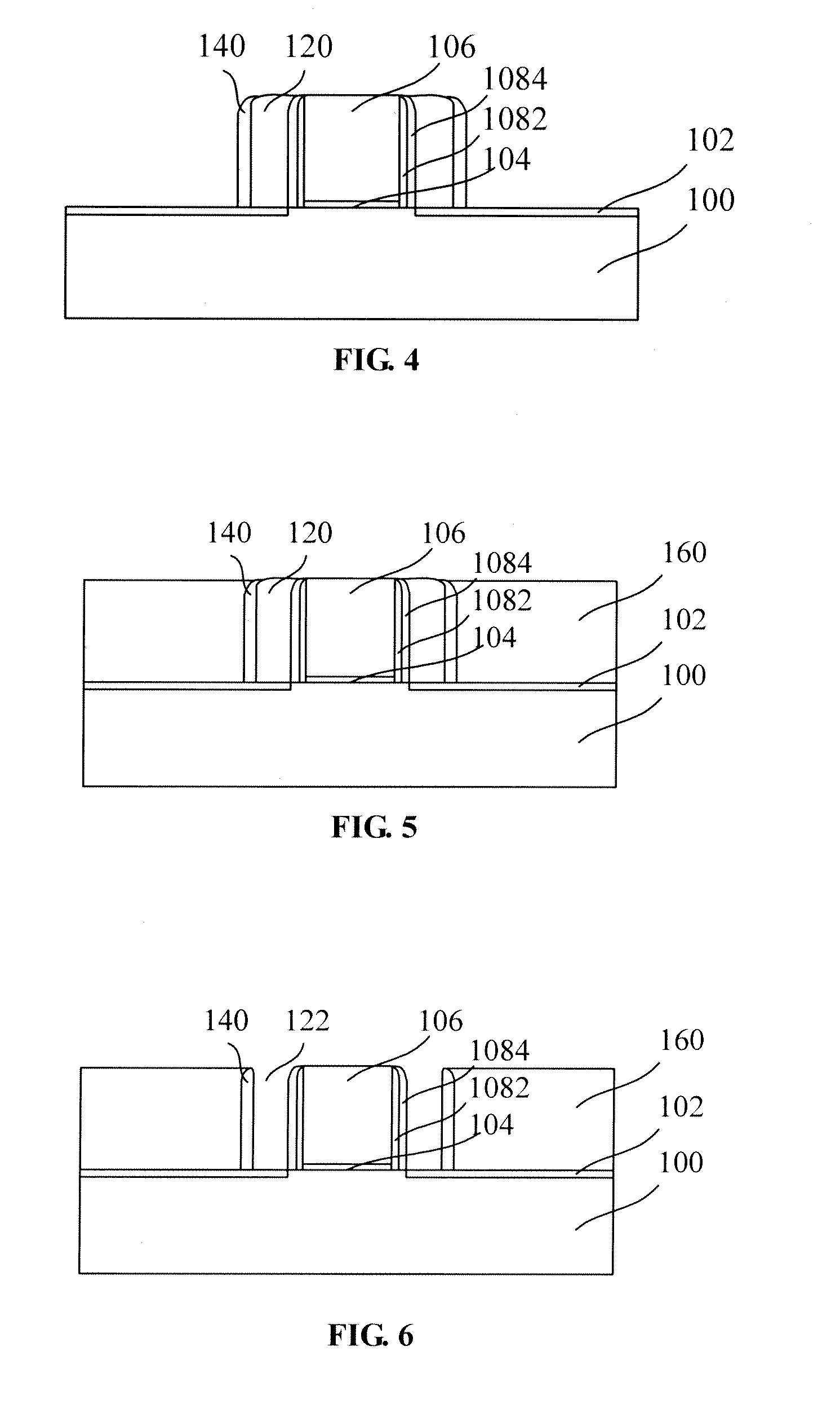
[0057]First, as shown in FIG. 4, a gate 106 (on a pre-formed gate dielectric layer 104), a sidewall spacer, a sacrificial sidewall spacer 120, a source region, a drain region (not shown), and an auxiliary sidewall spacer 140 are formed on a substrate 100. The sidewall spacer covers opposite sides of the gate 106, the sacrificial sidewall spacer 120 covers the sidewall spacer, the auxiliary sidewall spacer 140 covers side surfaces of the sacrificial sidewall spacer 120, and the source region and the drain region are within the substrate and on respective sides of the gate.

[0058]In this specification, the substrate 100 has undergone a processing operation, which comprises pre-cleaning, forming well regions and forming a shallow trench isolation (STI) region. In this embodiment, the substrate 100 is a silicon substrate. In other embodiments, the substrate 100 may comprise other compound ...

second embodiment

[0082]According to the invention, a method for forming a contact hole comprises the following steps.

[0083]First, as shown in FIG. 12, a gate stack 202, a sidewall spacer, a sacrificial sidewall spacer 206 and an auxiliary sidewall spacer 208 extending in a first direction are formed on a substrate 200. The sidewall spacer covers opposite sides of the gate stack 202, the sacrificial sidewall spacer 206 covers the sidewall spacer, and the auxiliary sidewall spacer 208 covers side surfaces of the sacrificial sidewall spacer 206.

[0084]The formation and materials of the substrate 200, the sidewall spacer (comprising a sidewall spacer base layer 2042 and a main sidewall spacer 2044), the sacrificial sidewall spacer 206 and the auxiliary sidewall spacer 208 are the same as those in the preceding embodiment, which are omitted here.

[0085]In the prior art, a method for forming a gate comprises the steps of: forming a gate stack 202 extending in a first direction, and then cutting the gate sta...


PUM


Abstract

The invention provides a method for forming a contact hole, comprising: forming a gate, a sidewall spacer, a sacrificial sidewall spacer, a source region and a drain region on a substrate, wherein the sidewall spacer is formed around the gate, the sacrificial sidewall spacer is formed over the sidewall spacer, and the source region and the drain region are formed within the substrate and on respective sides of the gate; forming an interlayer dielectric layer, with the gate, the sidewall spacer and the sacrificial sidewall spacer being exposed; removing the sacrificial sidewall spacer to form a contact space, a material that the sacrificial sidewall spacer is made of being different from any of materials that the gate, the sidewall spacer and the interlayer dielectric layer are made of; forming a conducting layer to fill the contact space; and cutting off the conducting layer, to form at least two conductors connected to the source region and the drain region respectively. The invention also provides a contact hole, the contact hole a gate and a sidewall spacer being formed on a substrate and within an interlayer dielectric layer, wherein the sides of the contact hole meet the sidewall spacer. The invention also provides a semiconductor device and a method for forming the same. With the technical solutions provided by the invention, the number of masks used can be reduced.

Description

CROSS REFERENCE TO RELATED APPLICATIONS[0001]The present application claims priority to PCT Application No. PCT / CN2011 / 071254, filed Feb. 24, 2011, which claimed priority to Chinese Patent Application No. 201010175815.5, entitled “CONTACT HOLE, SEMICONDUCTOR DEVICE AND METHOD FOR FORMING THE SAME”, filed May 14, 2010. Both the PCT application and the Chinese application are incorporated herein by reference in their entireties.FIELD OF THE INVENTION[0002]The present invention relates to the field of semiconductor technology, and in particular, to a contact hole, a semiconductor device and a method for forming the same.BACKGROUND OF THE INVENTION[0003]As the feature size of semiconductor devices is scaled, various microcosmic effects have been observed, resulting in more complex manufacturing processes of semiconductor devices, and difficulties in optimizing their performances. Complex manufacturing processes require more masks and multistage photolithography, and it has become a chal...

Claims


Application Information

Patent Timeline
IPC IPC(8): H01L21/336H01L21/283H01L21/3205
CPCH01L21/76831H01L21/76897H01L29/6656H01L29/6653H01L29/41783
Inventor ZHONG, HUICAIQINGQING, LIANG
Owner INST OF MICROELECTRONICS CHINESE ACAD OF SCI
Why Eureka
Try Eureka