Electronic device and manufacturing method therefor

a manufacturing method and electronic device technology, applied in the field of electronic devices, can solve the problems of further increase in the performance and functionality of electronic devices, process inevitably becomes complicated and time-consuming, and limit the high-density distribution of through-electrodes, etc., to achieve excellent high-frequency characteristics, high functionality, and high performance

Active Publication Date: 2011-11-24
NAPRA
View PDF8 Cites 32 Cited by
  • Summary
  • Abstract
  • Description
  • Claims
  • Application Information

AI Technical Summary

Benefits of technology

[0011]It is an object of the present invention to provide an electronic device having high performance, high functionality and excellent high-frequency characteristics and a manufacturing method therefor.

Problems solved by technology

However, since the distance between the through-electrodes has to be large in the structure where the ring-shaped, insulating isolation groove is provided to surround the through-electrode passing through the silicon substrate in a spaced apart relationship, there is a limit on high-density distribution of the through-electrodes and further increase in performance and functionality of the electronic device.
Moreover, since it requires the steps of forming a silicon film directly on the bottom face and the side faces of the isolation groove, forming an insulation film on the silicon film in such a manner as to fill up a gap left in the isolation groove after formation of the silicon film, and then thermally oxidizing the surface of the silicon film, the process inevitably becomes complicated and time-consuming.
When replacing the conventional planar arrangement with the TSV technology, cost performance is important from the viewpoint of industrial mass production, but the above related art cannot meet this need sufficiently.
This makes it difficult to form a silicon film in the isolation groove.
The TSV technology is applicable to a wide variety of electronic devices having the semiconductor substrate as a functional element, such as a sensor module, an optoelectronic module, a unipolar transistor, a MOS FET, a CMOS FET, a memory cell, integrated circuits (IC) thereof, various scales of LSIs, a light-emitting diode, and a solar cell, but the above-described problems occur in any case.

Method used


Image

  • Electronic device and manufacturing method therefor
  • Electronic device and manufacturing method therefor
  • Electronic device and manufacturing method therefor

Examples


Embodiment Construction

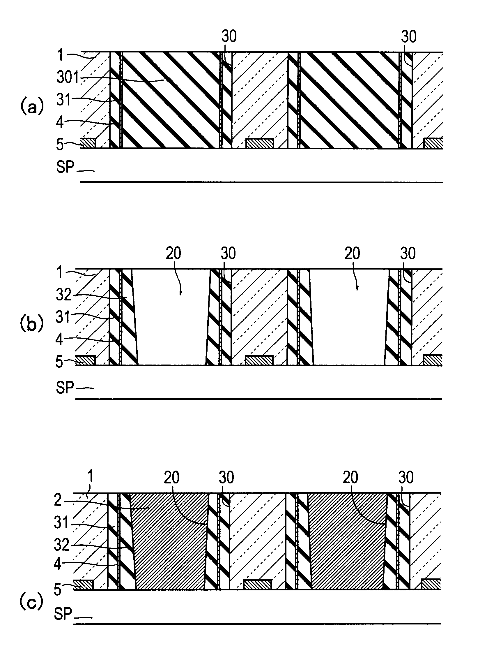
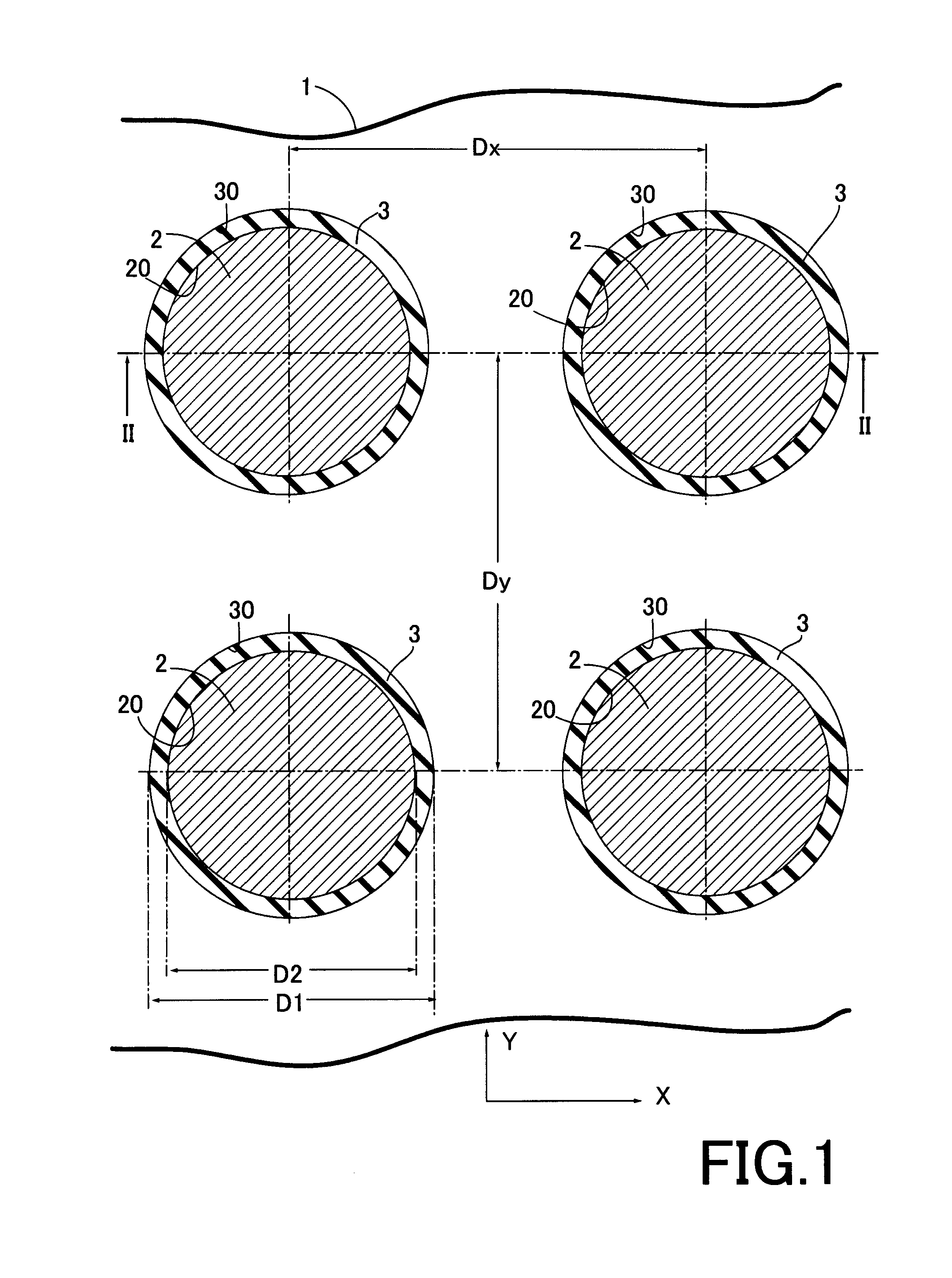
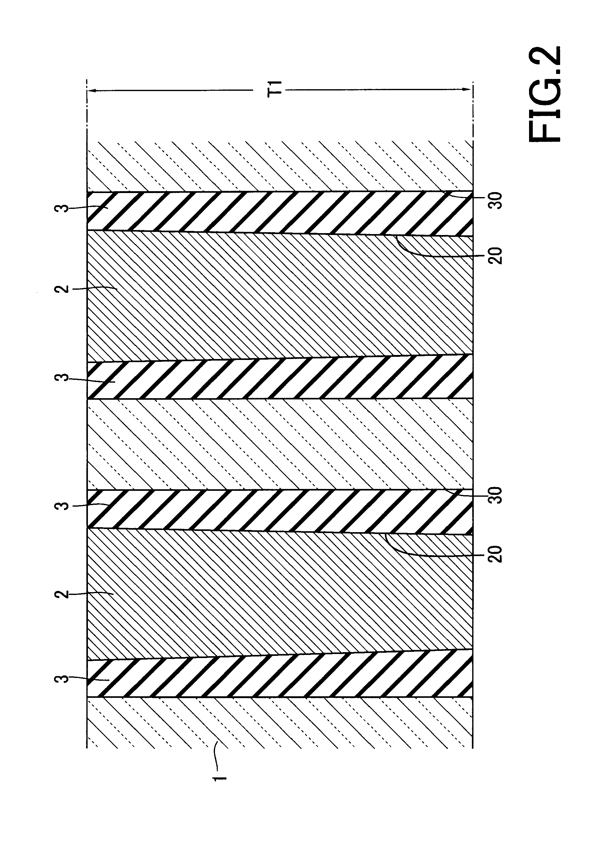
[0036]Referring to FIGS. 1 and 2, an interposer is illustrated as one embodiment of an electronic device according to the present invention. The interposer includes a semiconductor substrate 1, a vertical conductor 2 and an insulating material-filled layer 3. The semiconductor substrate 1 is, for example, a silicon substrate having a thickness T1 and in the form of a wafer or a chip cut out from the wafer. The thickness T1 may be, but not limited to, about 50 to 700 μm.

[0037]The semiconductor substrate 1 has a vertical hole 30 extending in a thickness direction thereof. The vertical holes 30 shown in the present embodiment pass through the semiconductor substrate 1 in the thickness direction with an inside diameter D1 and are arranged in rows, for example, in the form of matrix, as seen in an X-Y plane taken along the substrate surface, at a given arrangement pitch Dx, Dy in X, Y directions. However, the arrangement pitch Dx, Dy is not required to be constant, and the opening may ta...


PUM

PropertyMeasurementUnit
relative permittivityaaaaaaaaaa
thicknessaaaaaaaaaa

Abstract

An electronic device includes a semiconductor substrate, an insulating material-filled layer and a vertical conductor. The semiconductor substrate has a vertical hole extending in a thickness direction thereof. The insulating material-filled layer is a ring-shaped layer filled in the vertical hole for covering an inner periphery thereof and includes an organic insulating material or an inorganic insulating material mainly of a glass and a nanocomposite ceramic. The nanocomposite ceramic has a specific resistance of greater than 1014 Ω·cm at room temperature and a relative permittivity of 4 to 9. The vertical conductor is a solidified metal body filled in an area surrounded by the insulating material-filled layer.

Description

BACKGROUND OF THE INVENTION[0001]1. Field of the Invention[0002]The present invention relates to an electronic device and a manufacturing method therefor.[0003]2. Description of the Related Art[0004]Recently there has been proposed a TSV (through-silicon-via) technology of providing a semiconductor substrate such as a silicon substrate with a large number of through-electrodes. With the TSV technology, many functions can be packed into a small footprint, and important electrical pathways between elements can also be dramatically shortened to facilitate increasing processing speed.[0005]When using the TSV technology, the through-electrodes have to be electrically insulated from the silicon substrate. As means for electrical insulation, Japanese Unexamined Patent Application Publication No. 2008-251964 discloses a technology of forming a ring-shaped isolation groove passing through a silicon substrate in such a manner as to surround a through-electrode passing through the silicon subs...

Claims


Application Information

Patent Timeline
Patent Type & Authority Applications(United States)
IPC IPC(8): H01L33/62H01L21/28
CPCH01L23/481H01L2924/09701H01L2224/16146H01L2924/1461H01L2924/13091H01L21/76898H01L2224/13H01L2224/81H01L2924/00H01L23/48H01L23/045H01L23/055
Inventor SEKINE, SHIGENOBUSEKINE, YURINAKUWANA, YOSHIHARU
Owner NAPRA
Why Eureka
Try Eureka