
Methods and systems for laser processing a workpiece using a plurality of tailored laser pulse shapes

a laser pulse and workpiece technology, applied in the direction of manufacturing tools, electrical/magnetic/electromagnetic heating, welding/soldering/cutting articles, etc., can solve the problems of slow throughput, low mechanical strength of dies compared to mechanical sawing, and high material dependence, so as to increase the strength of die breakage

Inactive Publication Date: 2011-12-08
ELECTRO SCI IND INC
View PDF2 Cites 45 Cited by
  • Summary
  • Abstract
  • Description
  • Claims
  • Application Information

AI Technical Summary

Benefits of technology

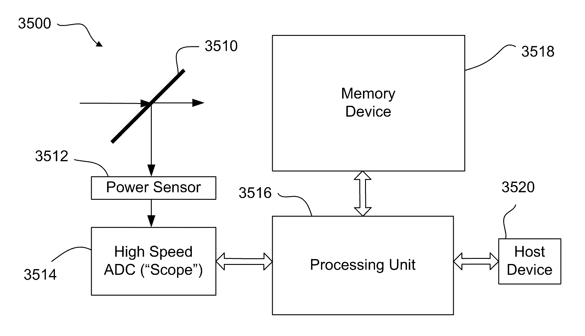
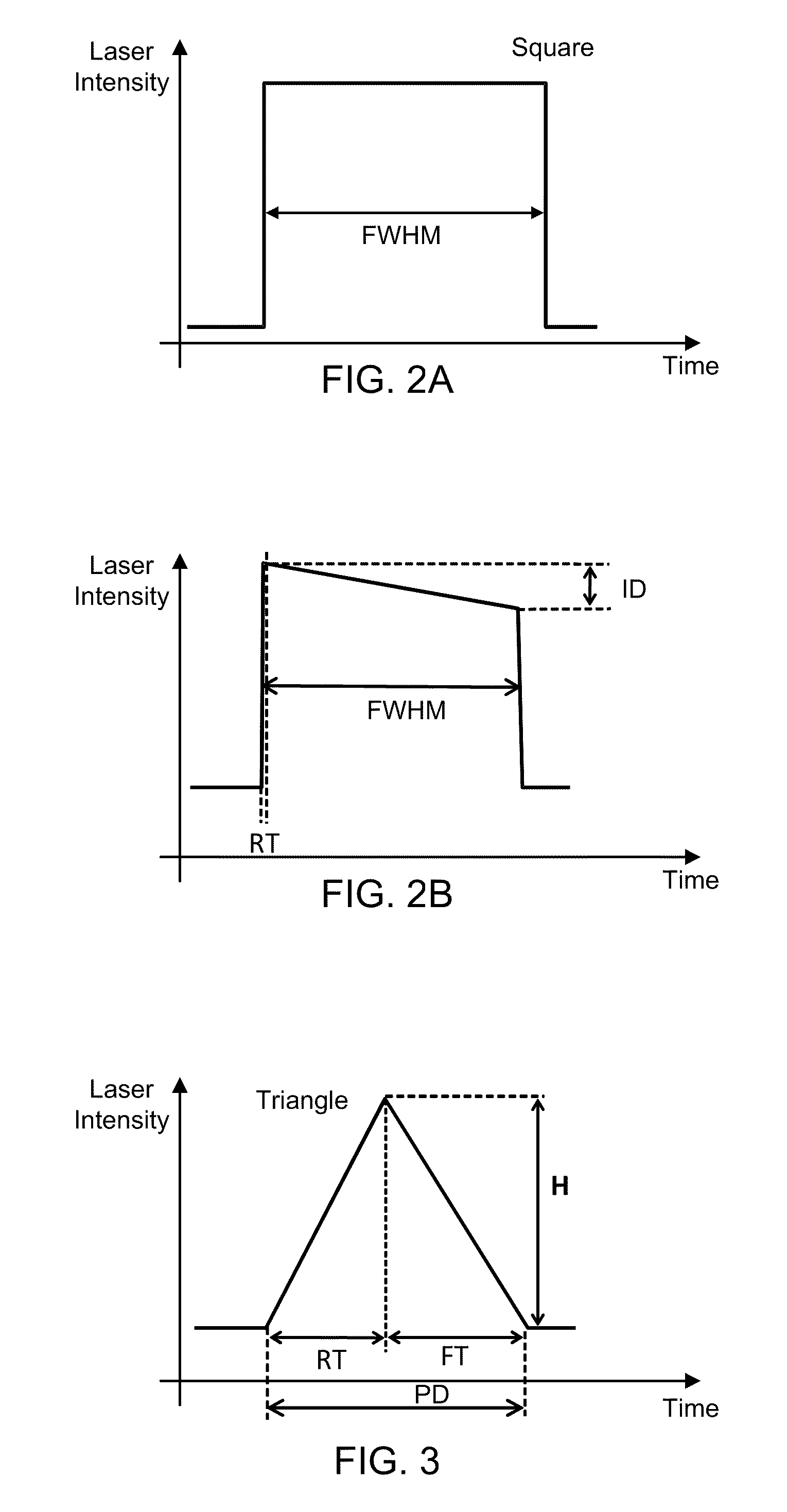
[0010]Tailored laser pulse shapes are used for processing workpieces. Laser dicing of semiconductor device wafers on die-attach film (DAF), for example, may use different tailored laser pulse shapes for scribing device layers down to a semiconductor substrate, dicing the semiconductor substrate, cutting the underlying DAF, and / or post processing of the upper die edges to increase die break strength. Different mono-shape laser pulse trains may be used for respective recipe steps or passes of a laser beam over a scribe line. In another embodiment, scribing a semiconductor device wafer includes only a single pass of a laser beam along a scribe line using a mixed-shape laser pulse train that includes at least two laser pulses that are different than one another. In addition, or in other embodiments, one or more tailored pulse shapes may be selected and provided to the workpiece on-the-fly. The selection may be based on sensor feedback.

Problems solved by technology

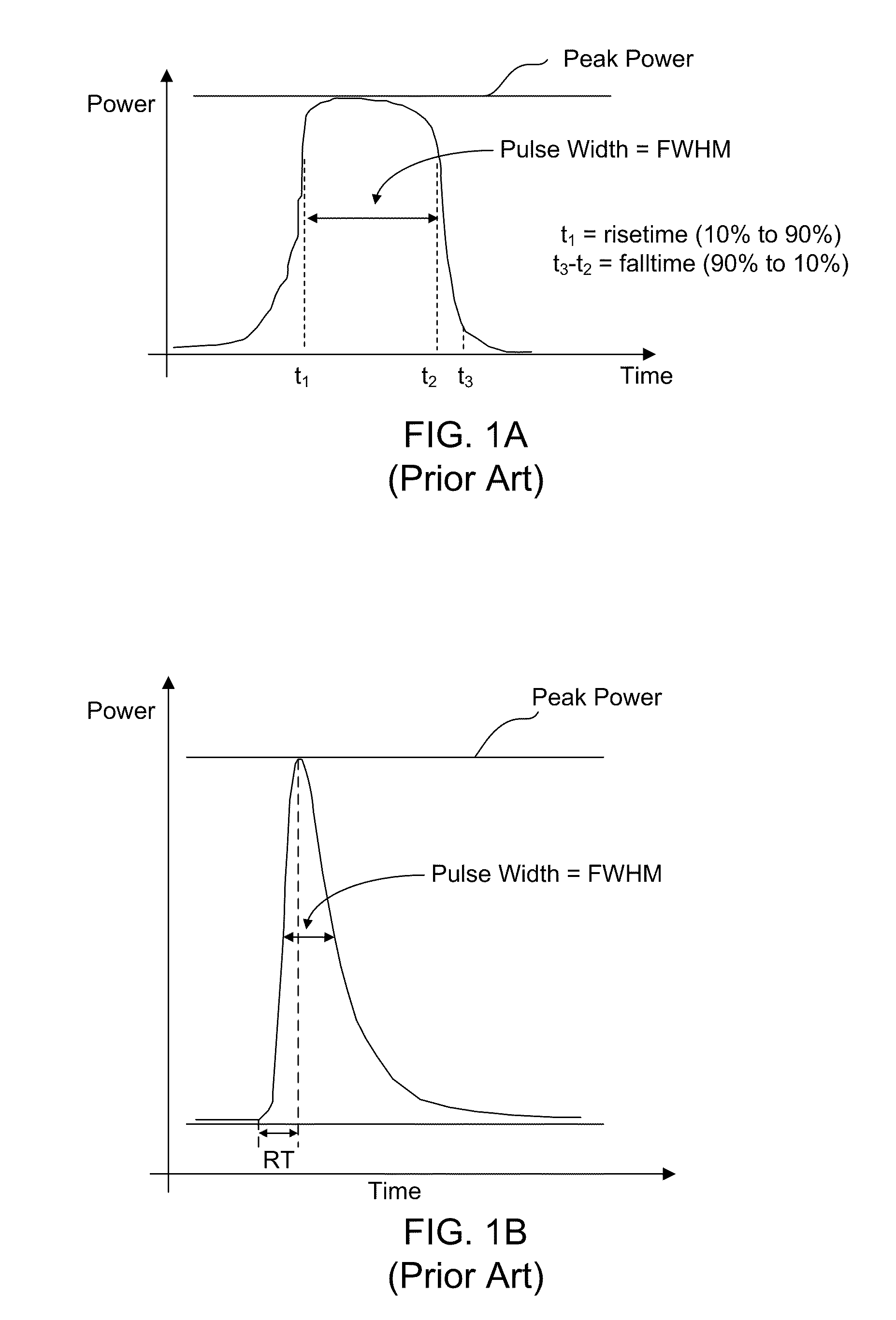
Generally, the pulse widths of laser pulses generated by such laser systems are functionally dependent on the PRF selected and are not independently adjustable based on differences between target structures or other process variables.
One problem for laser processing is that the results tend to be highly material dependent.
One example of a challenging problem is the singulation of semiconductor devices mounted on die attach film (DAF).
This problem is generally addressed in production by using mechanical diamond saws with ultra-thin blades because laser dicing with known processes tend to produce a die with lower mechanical strength compared to that produced by mechanical sawing.
Incorporation of fragile low-k dielectric materials into these semiconductor devices along with reduction of the silicon wafer thickness has increased the difficulty for mechanical saw dicing, leading to slower throughputs and more yield losses.

Method used


Image

  • Methods and systems for laser processing a workpiece using a plurality of tailored laser pulse shapes
  • Methods and systems for laser processing a workpiece using a plurality of tailored laser pulse shapes
  • Methods and systems for laser processing a workpiece using a plurality of tailored laser pulse shapes

Examples


Embodiment Construction

[0056]Laser micromachining systems and processes described herein provide high throughput laser micromachining of workpieces with good process results, including fast and efficient removal rates of materials, no chipping or cracking or other mechanical damage to the target material, control of material splash and ejected debris, no significant reduction in the material strength due to thermal damage or micro-cracking, and a process that meets cosmetic requirements (such as a smooth edge, smooth vertical or horizontal surfaces).

[0057]The term “tailored laser pulse” (also referred to herein as a shaped “temporal pulse profile”) refers to a laser pulse with an adjusted or programmed (shaped) laser power or intensity with respect to time (laser intensity vs. time). Thus, a tailored laser pulse or a shaped temporal pulse profile should not be confused with spatial shaping of laser pulses (such as a top-hat spatial beam shape). Skilled persons will recognize from the disclosure herein, ho...


PUM

PropertyMeasurementUnit
repetition frequencyaaaaaaaaaa
rise timeaaaaaaaaaa
fall time FTaaaaaaaaaa

Abstract

Tailored laser pulse shapes are used for processing workpieces. Laser dicing of semiconductor device wafers on die-attach film (DAF), for example, may use different tailored laser pulse shapes for scribing device layers down to a semiconductor substrate, dicing the semiconductor substrate, cutting the underlying DAF, and / or post processing of the upper die edges to increase die break strength. Different mono-shape laser pulse trains may be used for respective recipe steps or passes of a laser beam over a scribe line. In another embodiment, scribing a semiconductor device wafer includes only a single pass of a laser beam along a scribe line using a mixed-shape laser pulse train that includes at least two laser pulses that are different than one another. In addition, or in other embodiments, one or more tailored pulse shapes may be selected and provided to the workpiece on-the-fly. The selection may be based on sensor feedback.

Description

RELATED APPLICATION[0001]This application is a continuation-in-part of U.S. patent application Ser. No. 12 / 060,076, titled “Methods and Systems for Dynamically Generating Tailored Laser Pulses,” filed Mar. 31, 2008, which is hereby incorporated by references herein.TECHNICAL FIELD[0002]This disclosure relates to laser processing systems. In particular, this disclosure relates to laser systems and methods for micromachining (e.g., scribing or dicing) semiconductor devices and / or severing electrically conductive links with laser pulses having shaped temporal profiles.BACKGROUND INFORMATION[0003]Integrated circuits (ICs) are generally fabricated in an array on or in a semiconductor substrate. ICs generally include several layers formed over the substrate. One or more of the layers may be removed along scribing lanes or streets using a mechanical saw or a laser. After scribing, the substrate may be throughcut, sometimes called diced, using a saw or laser to separate the circuit componen...

Claims


Application Information

Patent Timeline
Patent Type & Authority Applications(United States)
IPC IPC(8): B29C35/08
CPCB23K26/063B23K26/0639H01L2924/13091H01L2924/0665H01L2924/01078H01L2924/01075H01L2924/01074H01L2924/01055B23K26/386B23K26/4075B23K26/409B23K26/426H01L21/6836H01L24/27H01L24/29H01L24/83H01L2221/68327H01L2224/27436H01L2224/2919H01L2224/83191H01L2924/01013H01L2924/01029H01L2924/01056H01L2924/0106H01L2924/01082H01S3/0057H01S3/102H01S3/1305H01L2924/01005H01L2924/01006H01L2924/01019H01L2924/01023H01L2924/01033H01L2924/00H01L2924/3512B23K26/064B23K26/705B23K26/0622B23K26/40H01L2924/12043H01L2924/14B23K26/389B23K2103/172B23K2103/50H01L21/30H01L21/78
Inventor HOOPER, ANDREWBARSIC, DAVIDBRULAND, KELLY J.FINN, DARAGH S.SHEEHAN, LYNNPENG, XIAOYUANOSAKO, YASUDUMESTRE, JIMJORDENS, WILLIAM J.
Owner ELECTRO SCI IND INC
Learn More