System and method for characterizing the electrical properties of a semiconductor sample

a semiconductor and electrical property technology, applied in the field of semiconductor characterization, can solve the problems of p-type gan, mocvd, and doped with p-type materials such as magnesium, which suffer from a notable drawback, and degrade the electronic properties of p-type gan

Inactive Publication Date: 2011-12-08
KAMIENIECKI EMIL
View PDF6 Cites 29 Cited by
  • Summary
  • Abstract
  • Description
  • Claims
  • Application Information

AI Technical Summary

Benefits of technology

[0020]It is yet another object of the present invention to provide a system and method as described above which allows for in-line process control and monitoring of the electrical characteristics of the semiconductor sample duri

Problems solved by technology

However, it has been found that, in general, GaN layers formed by growth methods, such as MOCVD, which is the predominant growth process in the HB-LED industry, and doped with p-type material such as magnesium, typically suffer from a notable drawback.
However, it has been found this relatively high level of “chemical” doping in turn degrades the electronic properties of the p-type GaN, which is highly undesirable.
As a second shortcoming, the requirement that the semiconductor wafer sample be cut into a number of smaller pieces in order to make a Hall measurement renders the overall process rather cumbersome and time-consuming to complete.
Since wide band gap semiconductors, such as GaN, have a doping, or acceptor, concentration that is often substantially higher (10 to 100 times higher) than its corresponding carrier concentration, the use of Hall measurements to characterize the crit

Method used


Image

  • System and method for characterizing the electrical properties of a semiconductor sample
  • System and method for characterizing the electrical properties of a semiconductor sample
  • System and method for characterizing the electrical properties of a semiconductor sample

Examples


Embodiment Construction

Semiconductor Characterization System 111

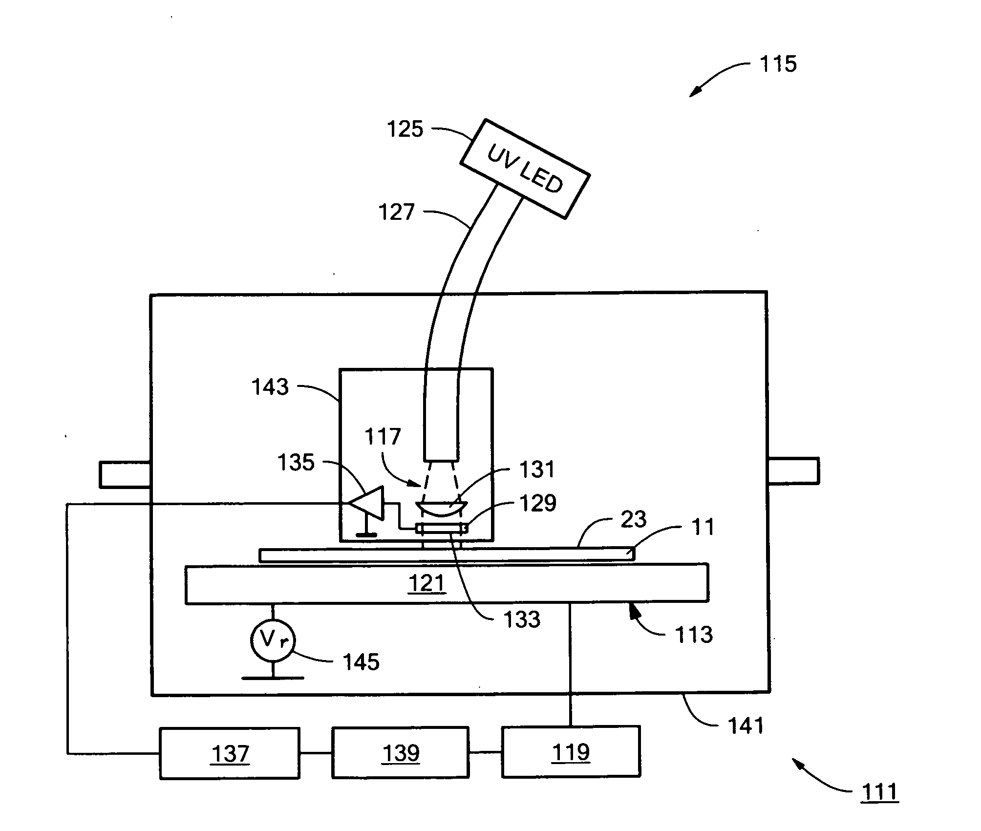
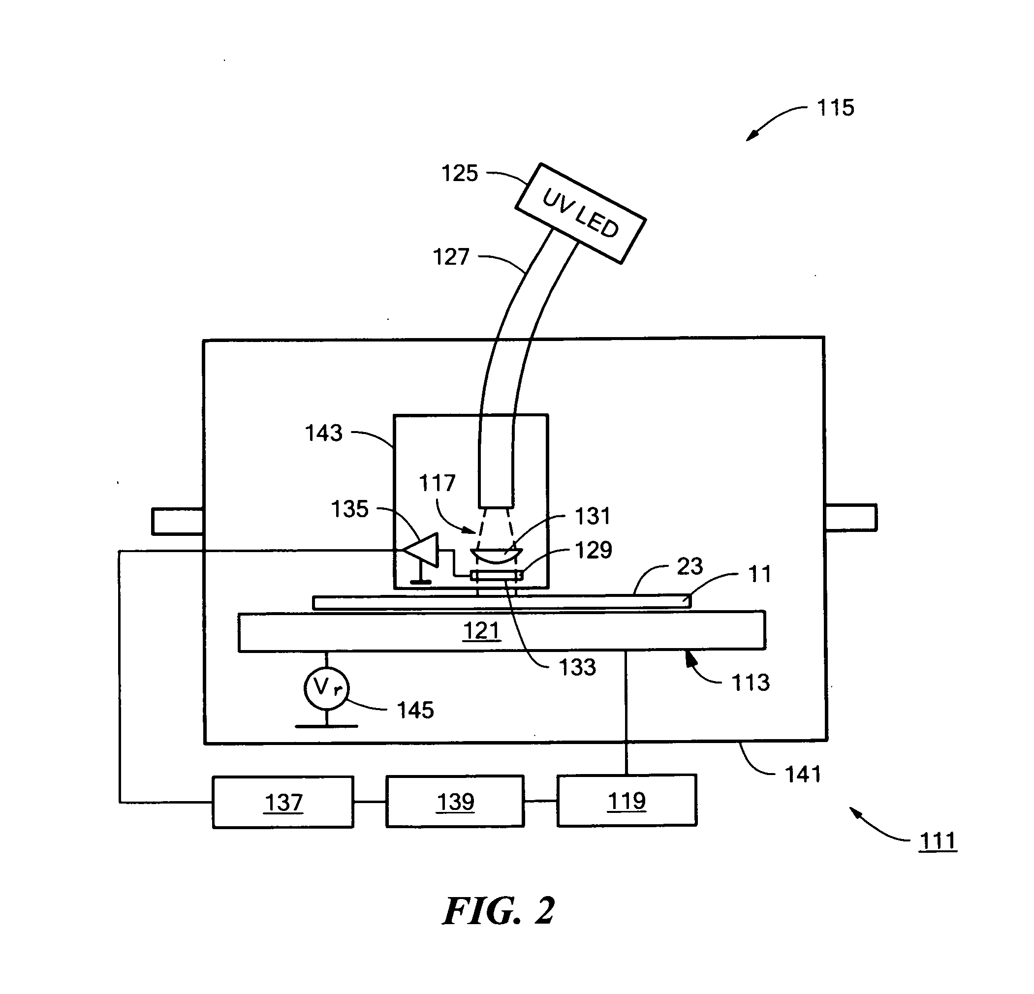
[0032]Referring now to FIG. 2, there is shown a system for characterizing the electrical properties of a semiconductor wafer structure, the system being constructed according to the teachings of the present invention and identified generally by reference numeral 111. As will be described in detail below, system 111 is principally designed to apply novel in-line, non-contact surface photovoltage (SPV) techniques to semiconductor wafer structures with high surface state densities, which is a principal object of the present invention. Although conventional surface photovoltage techniques are not typically applied to semiconductor wafer structures with high surface state densities, such as GaN, due to the inherent electrostatic shielding of the interior of the top layer (e.g., the subsurface region 25 of top cladding layer 19) from the externally applied voltage or charge, it is to be understood that the system and method of the present invention...


PUM


Abstract

A system for characterizing the electrical properties of semiconductor wafers with high surface state densities, such as GaN wafers, includes a support subsystem for supporting the semiconductor sample, at least one light source for illuminating a spot on the sample, and a detection subsystem for measuring the photovoltage signal produced from illumination of the sample. In use, the system utilizes in-line, non-contact photovoltage techniques that exploits the presence of the high surface state density and the known components of its associated electrostatic barrier as part of its novel characterization process. Specifically, the system illuminates the sample with one or more light beams that vary in photon energy and duration in order to excite charge carriers in specific layers of the sample while either preserving or collapsing the electrostatic barrier. In this manner, the system is able to electrically characterize individual or combined layers of the sample as well as embedded junctions.

Description

CROSS-REFERENCE TO RELATED APPLICATIONS[0001]The present application claims the benefit under 35 U.S.C. 119(e) of U.S. provisional patent application Ser. No. 61 / 396,853, filed Jun. 3, 2010, the disclosure of which is incorporated herein by reference.TECHNICAL FIELD[0002]The present invention relates generally to semiconductor characterization and more particularly to systems and methods for determining basic electrical parameters of the thin films and layers that form multi-layer semiconductor wafer structures.BACKGROUND ART[0003]Semiconductors are well known in the art and are commonly used in the manufacture of a wide variety of electronic devices including light emitting diodes, lasers, photo-detectors, transistors, solar cells, diodes, silicon controlled rectifiers and integrated circuits. Semiconductors are commonly constructed as wafers using one or more types of semiconducting materials, such as silicon, germanium, gallium arsenide and silicon carbide.[0004]Due to its unique...

Claims


Application Information

Patent Timeline
IPC IPC(8): G01R29/00G06F19/00
CPCG01R31/2656G01R31/2648
Inventor KAMIENIECKI, EMIL
Owner KAMIENIECKI EMIL
Why Eureka
Try Eureka