Process for producing photovoltaic device and photovoltaic device

Inactive Publication Date: 2011-12-15
MITSUBISHI HEAVY IND LTD
View PDF2 Cites 3 Cited by
  • Summary
  • Abstract
  • Description
  • Claims
  • Application Information

AI Technical Summary

Benefits of technology

[0014]The gas flow rate and the substrate temperature readily develop a distribution within the substrate plane as the surface area of the substrate is increased. Furthermore, if the substrate develops warping, then the substrate-electrode separation distance tends to also vary within the substrate plane. When a photovoltaic device is produced using the production process of the present invention, because the process exhibits a high degree of robustness relative to fluctuations within the substrate plane of the total gas flow rate, the substrate temperature and the substrate-electrode separation distance, variations in the film quality and performance (photovoltaic conversion efficiency) can be suppressed even if a substrate in-plane distribution develops for one or more of the above deposition conditions. As a result, the electric power output per photovoltaic device can be improved.
[0015]Moreover, the gas flow rate and the effective supplied electric power is prone to fluctuations between production batches or lots. If the production process of the present invention is used, then because the process exhibits a high degree of robustness relative to fluctuations in the total gas flow rate and the supplied electric power, even if the gas flow rate and/or supplied electric power fluctuates between batches or between lots, the effect of such fluctuations on changes in the film quality the photovolatic conversion efficiency can be minimized. As a result, variations i

Problems solved by technology

Further, fluctuations in the deposition conditions also occur between production lots.
Fluctuations in the deposition conditions within the substrate plane tend to be particularly problematic when a large surface area substrate with a substrate surface area of at l

Method used


Image

  • Process for producing photovoltaic device and photovoltaic device
  • Process for producing photovoltaic device and photovoltaic device
  • Process for producing photovoltaic device and photovoltaic device

Examples


Embodiment Construction

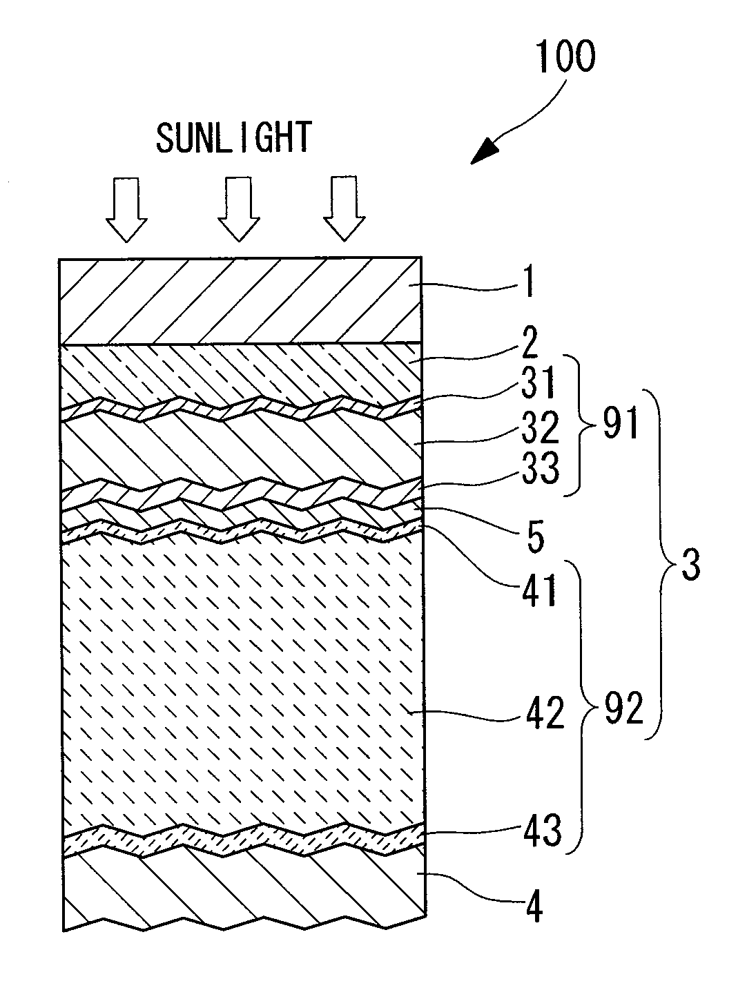
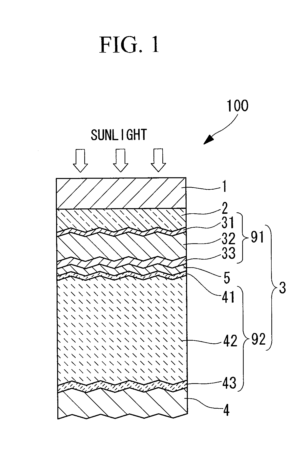
[0058]FIG. 1 is a schematic representation illustrating the structure of a photovoltaic device according to the present invention. A photovoltaic device 100 is a tandem silicon-based solar cell, and comprises a substrate 1, a transparent electrode layer 2, a first cell layer 91 (amorphous silicon-based) and a second cell layer 92 (crystalline silicon-based) as a photovoltaic layer 3, an intermediate contact layer 5, and a back electrode layer 4. Here, the term “silicon-based” is a generic term that includes silicon (Si), silicon carbide (SiC) and silicon germanium (SiGe). Further, the term “crystalline silicon-based” describes a silicon system other than an amorphous silicon system, and includes both microcrystalline silicon systems and polycrystalline silicon systems.

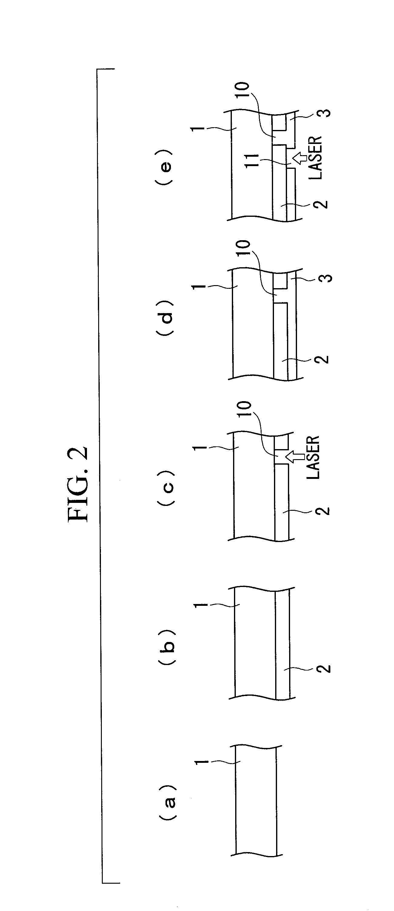
[0059]An embodiment in which the production process according to the present invention is applied to the deposition of a crystalline silicon i-layer is described below, using the production steps for a solar cell panel...


PUM

PropertyMeasurementUnit
Fractionaaaaaaaaaa
Speedaaaaaaaaaa
Speedaaaaaaaaaa

Abstract

A process for producing a photovoltaic device that suppresses variations in the photovoltaic conversion efficiency within the plane of a large surface area substrate, suppresses fluctuations in the module power output between production lots, and enables an improvement in the productivity. A process for producing a photovoltaic device that includes forming a silicon-based photovoltaic layer on a substrate using a plasma enhanced CVD method that employs a gas containing a silane-based gas and hydrogen gas as the raw material gas, under conditions in which the flow rate of the hydrogen gas per unit surface area of the substrate is not less than 80 slm/m2.

Description

TECHNICAL FIELD [0001]The present invention relates to a photovoltaic device, and relates particularly to a process for producing a thin-film silicon-based solar cell in which the electric power generation layer is formed by deposition, and a photovoltaic device prepared using this production process.BACKGROUND ART [0002]One known example of a photovoltaic device that converts the energy from sunlight into electrical energy is a thin-film silicon-based solar cell comprising a photovoltaic layer formed by using a plasma enhanced CVD method or the like to deposit thin films of a p-type silicon-based semiconductor (p-layer), an i-type silicon-based semiconductor (i-layer) and an n-type silicon-based semiconductor (n-layer). Advantages of thin-film silicon-based solar cells include the comparative ease with which the surface area can be increased, and the fact that the film thickness is approximately 1 / 100th that of a crystalline solar cell, meaning minimal material is required. As a re...

Claims


Application Information

Patent Timeline
IPC IPC(8): H01L31/0264H01L31/18H01L31/04H01L31/06H01L31/077
CPCC23C16/24H01L21/02529H01L21/02532H01L21/0262H01L31/076H01L31/1804H01L31/0463H01L31/1824H01L31/202Y02E10/545Y02E10/546Y02E10/548Y02E10/547H01L31/182Y02P70/50
Inventor GOYA, SANEYUKISAKAI, SATOSHI
Owner MITSUBISHI HEAVY IND LTD
Why Eureka
Try Eureka