Ferroelectric Memories based on Arrays of Autonomous Memory Bits

Active Publication Date: 2011-12-15
RADIANT TECH
View PDF5 Cites 16 Cited by
  • Summary
  • Abstract
  • Description
  • Claims
  • Application Information

AI Technical Summary

Benefits of technology

[0054]Switch 128 can be implemented with any element or arrangement of elements that provides an impedance between first and second terminals that varies as a function of the potential on a control terminal. Exemplary embodiments of switch 128 include transistors, both bi-polar and field effect, ferroelectric field effect transistors, relays, or circuits constructed from a plurality of such elements. Ferroelectric FETs are known to the art, and hence, will not be discussed in detail here. The reader is directed to U.S. Pat. No. 5,070,385 for a more detailed description of these devices. A ferroelectric FET can be fabricated in the same fabrication system as ferroelectric capacitor 127 allowing them to be built simultaneously at reduced cost. It should also be noted that the ferroelectric devices do not require a crystalline substrate such as a silicon wafer. The devices can be fabricated on any substrate that can withstand the fabrication temperatures, and hence, the entire circuit can be fabricated on a non-crystalline substrate, which substantially reduces the cost of fabrication. Since size is an important factor in many memories, switches based on single devices are preferred in such memories.

Problems solved by technology

However, these memories have a number of drawbacks.
First, the cost of these memories is still an order of magnitude greater than the cost of a conventional disk drive having the same capacity.
Unfortunately, the time needed to write a memory cell limits the rate at which data can be written to the memory to times that are significantly longer than the write times for conventional high-speed disk drives.
Second, the number of write cycles that can be executed on each cell before the memory fails is significantly less than that of conventional disk drives.
Third, the cost of providing a semiconductor disk drive that has write times that are as good or better than the fastest conventional disk drives further increases the cost of the drives to the point where one drive can cost more than a conventional personal computer system.
Finally, flash memory is confined to silicon fabrication regimes that are not easily adapted to environments in which high energy x-rays or other high-energy radiation is present.
Hence, these memories are not useful in such high radiation environments.
Since the amount of charge that is released is large when the dielectric in the ferroelectric capacitor state flips, the bit line circuitry presents challenges.
Furthermore, the readout operation destroys the data if the cell is in the state in which the polarization flips; hence, the contents of the memory cell must be re-written each time the cell is read, which further complicates the bit line circuitry.
Unfortunately, the silicon area needed to implement a conventional ferroelectric latch memory cell is much greater than that needed to implement the one capacitor, one transistor cell described above.

Method used


Image

  • Ferroelectric Memories based on Arrays of Autonomous Memory Bits
  • Ferroelectric Memories based on Arrays of Autonomous Memory Bits
  • Ferroelectric Memories based on Arrays of Autonomous Memory Bits

Examples


Embodiment Construction

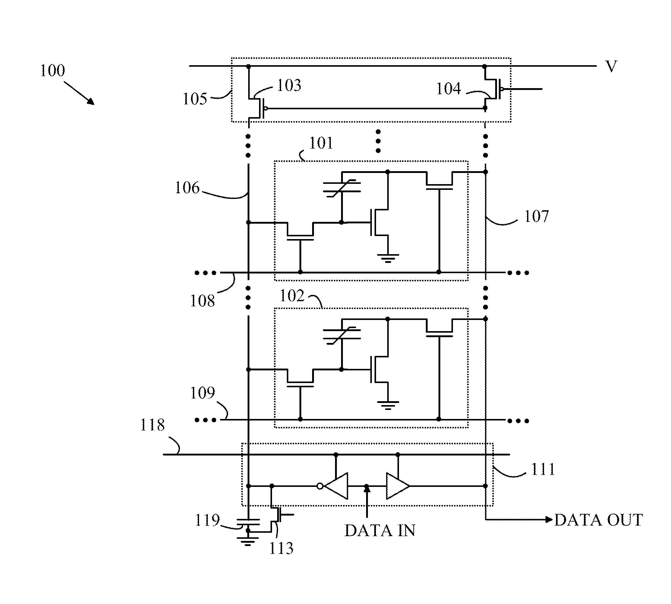
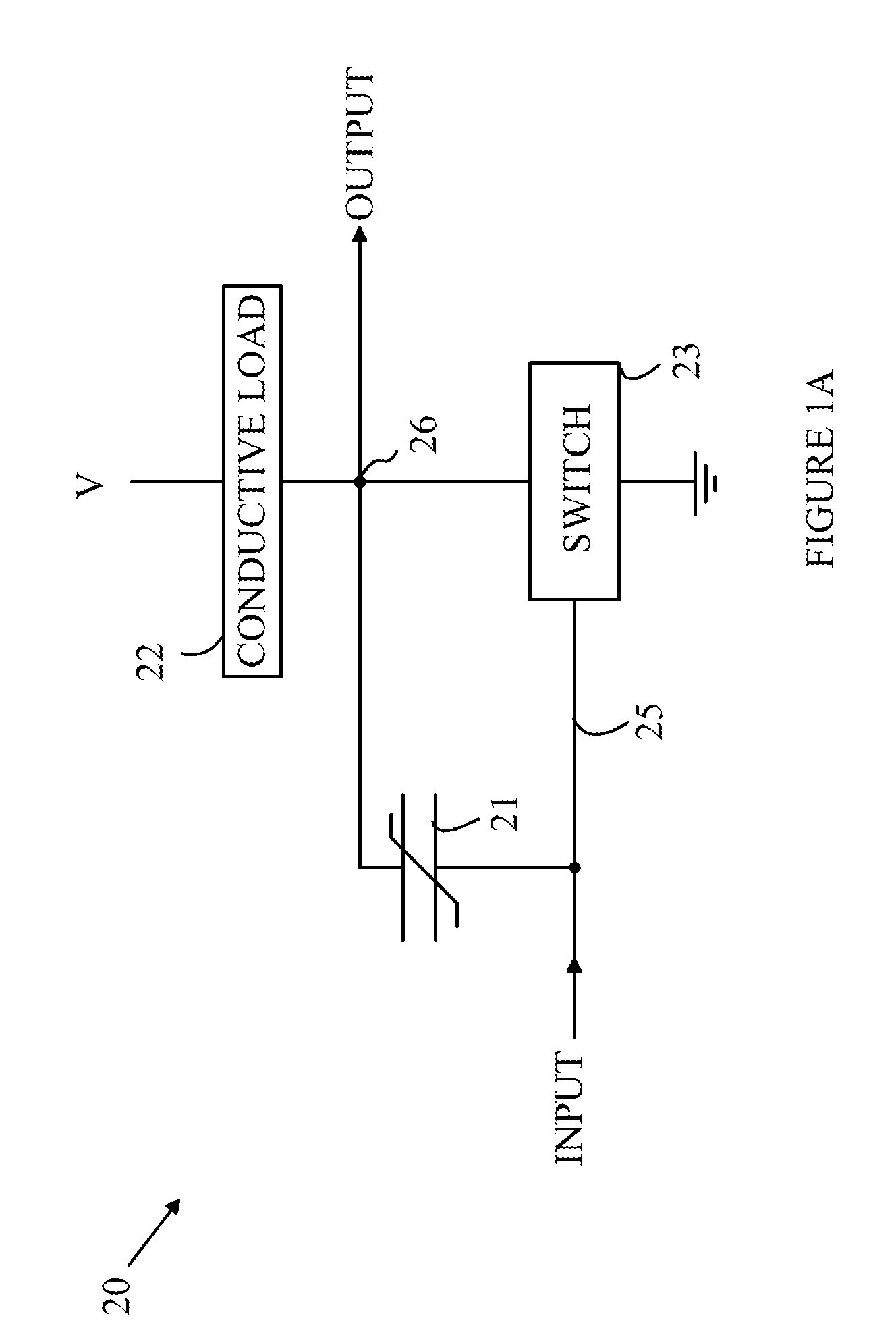
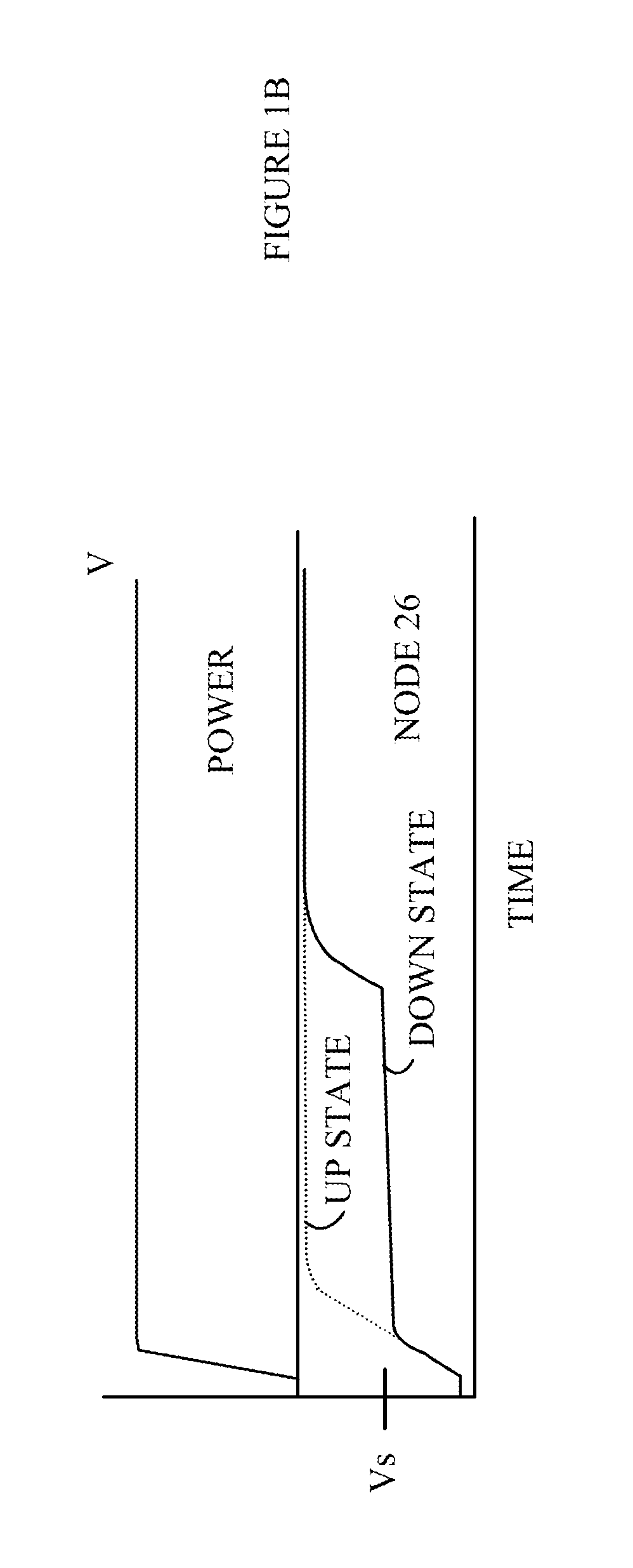
[0023]The manner in which the present invention provides its advantages can be more easily understood with reference to a novel ferroelectric latch design that is described in co-pending application U.S. Ser. No. 12 / 480,645, which is hereby incorporated by reference. The latch is constructed from an autonomous memory circuit and a feedback loop. Refer first to FIG. 1A, which is a schematic drawing of an autonomous memory circuit. Autonomous memory circuit 20 includes a ferroelectric capacitor 21 and a switch 23 having a current actuated control input 25. A conductive load 22 is connected between a power rail and switch 23.

[0024]Ferroelectric capacitor 21 has a remanent polarization that can be switched by applying a voltage across ferroelectric capacitor 21. That is, in the absence of a voltage across the capacitor, the dielectric of the capacitor is electrically polarized. The dielectric has two states corresponding to the dielectric being polarized either up or down. If a voltage ...


PUM


Abstract

A memory having a plurality of ferroelectric memory cells connected between first and second bit lines is disclosed. A read circuit is also connected between the first and second bit lines. A word select circuit selects one of the ferroelectric memory cells and generates a potential on the first hit line indicative of a value stored in the selected one of the plurality of ferroelectric memory cells. Each ferroelectric memory cell includes a ferroelectric capacitor and a variable impedance element having an impedance between first and second switch terminals that is determined by a signal on a control terminal. The ferroelectric capacitor is connected between the control terminal and the first switch terminal. First and second gates connect the ferroelectric memory cell to the bit lines in response to the word select circuit selecting that ferroelectric memory cell.

Description

BACKGROUND OF THE INVENTION[0001]Semiconductor based non-volatile memories are useful both in terms of data storage and as an alternative to rotating disk memories. Memories based on flash EEPROM cells have found increasing applications in computers as well as consumer devices such as cameras, mp3 players, and PDAs. The cost of flash EEPROM memories has decreased to the point that such memories are being used as a replacement for disk drives in computers. Semiconductor disk drives are particularly attractive for laptop computers because they require significantly lower power, are shock resistant, and are typically faster than the conventional disk drives that are utilized in such systems.[0002]However, these memories have a number of drawbacks. First, the cost of these memories is still an order of magnitude greater than the cost of a conventional disk drive having the same capacity. In one class of memory, one bit is stored in each memory cell. The memory cell includes an EEPROM ce...

Claims


Application Information

Patent Timeline
IPC IPC(8): G11C11/22G11C7/00G11C11/24
CPCG11C11/22
Inventor EVANS, JR., JOSEPH TATE
Owner RADIANT TECH
Why Eureka
Try Eureka