Method and data transceiving system for generating reference clock signal

a data transceiving system and clock signal technology, applied in the direction of digital transmission, pulse automatic control, synchronisation signal speed/phase control, etc., can solve the problems of occupying a larger space on the circuit board and the cost of crystal devices

Active Publication Date: 2011-12-22
PHISON ELECTRONICS
View PDF8 Cites 19 Cited by
  • Summary
  • Abstract
  • Description
  • Claims
  • Application Information

AI Technical Summary

Benefits of technology

[0011]In one embodiment of the present invention, the frequency lock controller increases a value of the voltage adjusting signal when receiving the logic high signal, so as to control the voltage controlled oscillator to increase the clock frequency of the reference clock signal; and reducing the value of the voltage adjusting signal when receiving the logic low signal, so as to control the voltage controlled oscillator to reduce the clock frequency of the reference clock signal.
[0013]In one embodiment of the present invention, the frequency lock controller compares a count of the SOF signals with a standard value, increases a value of the voltage adjusting signal when the count is smaller than the standard value, so as to control the voltage controlled oscillator to increase the clock frequency of the reference clock signal, and reduces the value of the voltage adjusting signal when the count is larger than the standard value, so as to control the voltage controlled oscillator to reduce the clock frequency of the reference clock signal.
[0018]Based on the above, the method and the data transceiving system for generating a reference clock signal of the present invention dispose a voltage controlled oscillator in the integrated chip to generate a reference clock signal and use the clock signal of the received input data stream to correct the frequency of the reference clock signal. The correction is feedback to the voltage controlled oscillator to adjust the clock frequency of the reference clock signal generated by the voltage controlled oscillator, such that the clock frequency of the PLL clock signal generated by the PLL unit can be locked to the clock frequency of the clock signal of the input data stream. Accordingly, the present invention is able to generate a PLL clock signal with accurate frequency without using a crystal device.

Problems solved by technology

Although a commercial crystal device may provide a clock signal with the frequency error less than 100 ppm and can serve as an ideal clock signal source, this kind of crystal device usually costs a lot and occupies a larger space of the circuit board.

Method used


Image

  • Method and data transceiving system for generating reference clock signal
  • Method and data transceiving system for generating reference clock signal
  • Method and data transceiving system for generating reference clock signal

Examples


first embodiment

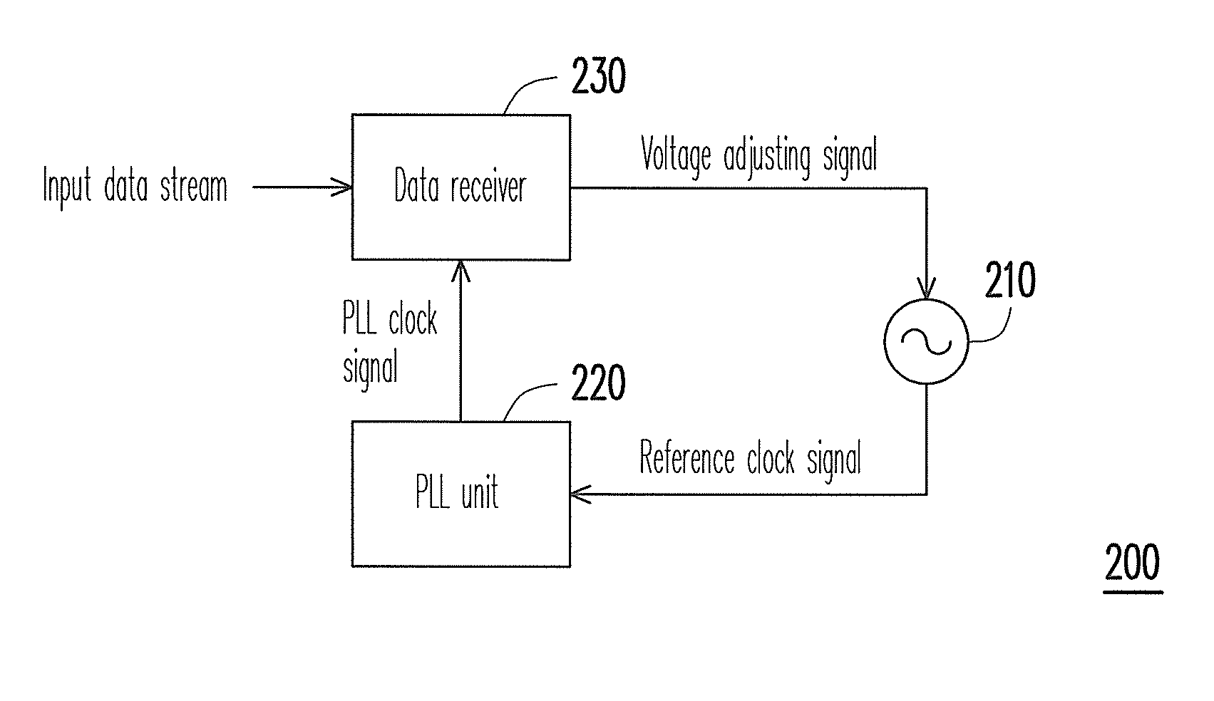
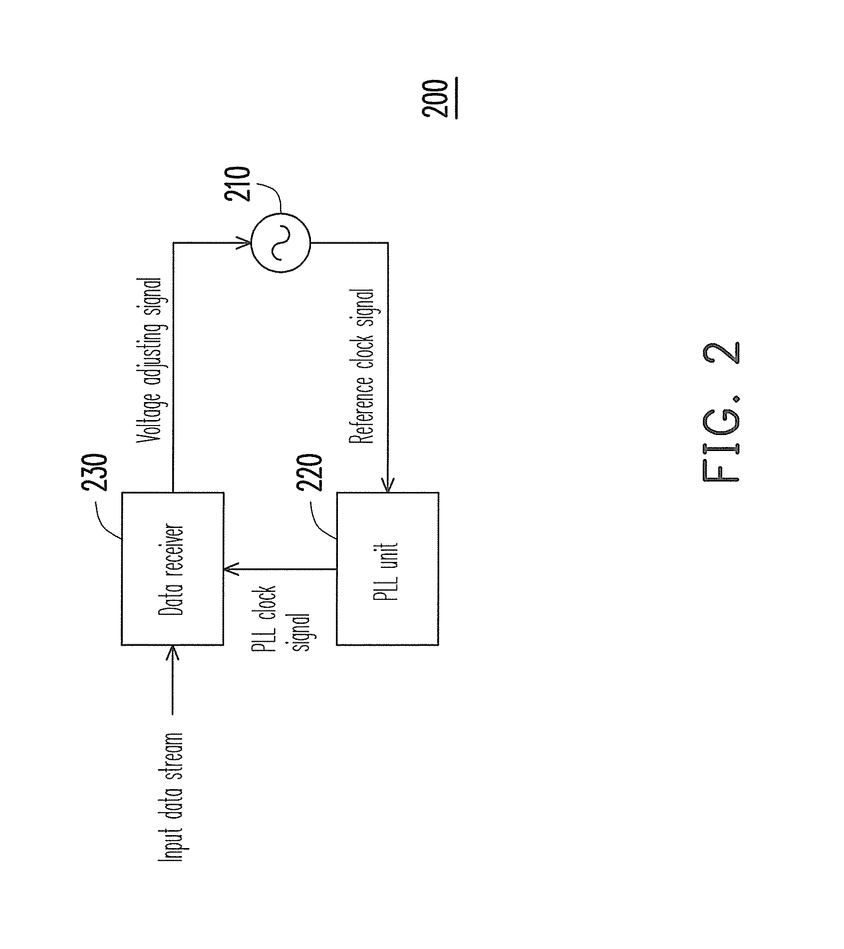
[0031]FIG. 2 is a block diagram of a data transceiving system for generating a reference clock signal according to first embodiment of the present invention. Referring to FIG. 2, the data transceiving system 200 of the present embodiment comprises a voltage controlled oscillator 210, a PLL unit 220 and a data receiver 230, and the functions thereof are respectively described in the following.

[0032]The voltage controlled oscillator 210 is, for example, a resistance / capacitance (RC) oscillator, a ring oscillator, or an inductance / capacitance (LC) oscillator for generating a reference clock signal.

[0033]The PLL unit 220 is coupled to the voltage controlled oscillator 210 and is used for outputting a PLL clock signal having a predetermined frequency and phase by using the reference clock signal outputted by the voltage controlled oscillator 210.

[0034]In the present embodiment, the PLL unit 220 is implemented in a digital means. For example, FIG. 3 is an example of a PLL unit according t...

second embodiment

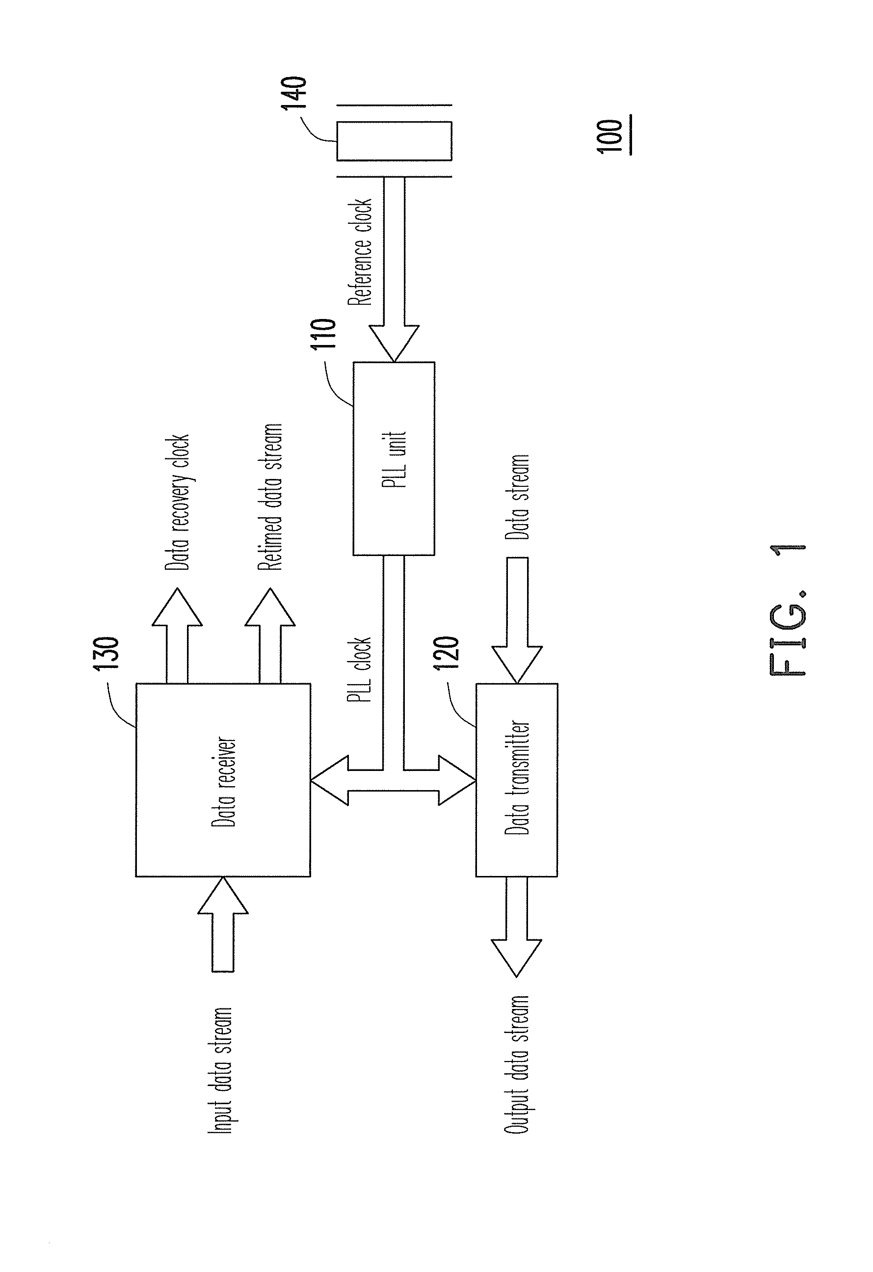
[0039]FIG. 5 is a block diagram of a data transceiving system for generating a reference clock signal according to second embodiment of the present invention. FIG. 6 is flowchart illustrating a method for generating a reference clock signal according to second embodiment of the present invention. Referring to both FIG. 5 and FIG. 6, the data transceiving system 500 of the present embodiment comprises a voltage controlled oscillator 510, a PLL unit 520, a data receiver 530, a digital-to-analog converter 540, and a data transmitter 550, in which the data receiver 530 further comprises a frequency detector 532 and a frequency lock controller 534. Detailed steps of the method for generating the reference clock signal of the present invention are described with the elements described in the above.

[0040]First, the voltage controlled oscillator 510 generates a reference clock signal (step S602). The voltage controlled oscillator 210 is, for example, a resistance / capacitance (RC) oscillator...

third embodiment

[0052]On the other hand, the present invention also uses tokens of the SOF defined in the specification of universal serial bus (USB) 2.0 to compare the PLL clock signal with the clock signal of the input data stream, so as to adjust the clock frequency of the reference clock signal generated by the voltage controlled oscillator.

[0053]FIG. 7 is a block diagram of a data transceiving system for generating a reference clock signal according to third embodiment of the present invention. FIG. 8 is flowchart illustrating a method for generating a reference clock signal according to third embodiment of the present invention. Referring to both FIG. 7 and FIG. 8, the data transceiving system 700 of the present embodiment comprises a voltage controlled oscillator 710, a PLL unit 720, a data receiver 730, a digital-to-analog converter 740, and a data transmitter 750, in which the data receiver 730 further comprises a clock and data recovery circuit 732, a SOF decoder 734, and a frequency lock...


PUM


Abstract

A method and a data transceiving system for generating a reference clock signal are provided. The data transceiving system comprises a voltage controlled oscillator, a phase lock loop (PLL) unit, and a data receiver. The voltage controlled oscillator is used to generate a reference clock signal. The PLL unit is used to increase a clock frequency of the reference clock signal to generate a PLL clock signal. The data receiver is used to compare the PLL clock signal with a clock signal of an input data stream, so as to output a voltage adjusting signal to the voltage controlled oscillator. The voltage controlled oscillator adjusts the clock frequency of the reference clock signal to be generated according to the reference clock signal, so as to lock the clock frequency of the PLL clock signal to a base frequency of the clock signal of the input data stream.

Description

CROSS-REFERENCE TO RELATED APPLICATION[0001]This application claims the priority benefit of Taiwan application serial no. 99120274, filed on Jun. 22, 2010. The entirety of the above-mentioned patent application is hereby incorporated by reference herein and made a part of specification.BACKGROUND OF THE INVENTION[0002]1. Field of the Invention[0003]The present invention is related to a data transceiving system, and more particularly, to a method and a data transceiving system for generating a reference clock signal.[0004]2. Description of Related Art[0005]FIG. 1 illustrates a structure of a data transceiver of a conventional integrated chip. The data transceiver 100 comprises a phase lock loop (PLL) unit 110, a data transmitter (TX) 120, and a data receiver (RX) 130 having a function of clock data recovery (CDR). The integrated chip generates a clock signal having an accurate frequency (i.e. less than tens ppm deviating from a target frequency) by using a crystal device 140, and use...

Claims


Application Information

Patent Timeline
Patent Type & Authority Applications(United States)
IPC IPC(8): H04L7/00
CPCH03L7/087H04L7/04H04L7/033H03L7/093
Inventor CHEN, AN-CHUNGCHENG, WEN-LUNGCHEN, WEI-YUNG
Owner PHISON ELECTRONICS
Why Eureka
Try Eureka