Method for manufacturing liquid crystal display panels

a technology of liquid crystal display panel and continuous manufacturing, which is applied in the direction of lamination ancillary operations, instruments, chemistry apparatus and processes, etc., to achieve the effect of less more susceptible to electrostatic decay, and rapid attenuation

Active Publication Date: 2011-12-29
NITTO DENKO CORP
View PDF1 Cites 18 Cited by
  • Summary
  • Abstract
  • Description
  • Claims
  • Application Information

AI Technical Summary

Benefits of technology

[0079]The first polarizing plate 10 includes at least a first polarizer 11 (having an absorption axis in a direction parallel to the short side of the liquid crystal cell 4). The first polarizing plate 10 includes the first polarizer 11; first and second protective films 13 and 14 placed on both sides of the first polarizer 11, wherein the first protective film is closer to the liquid crystal cell; a first electrically-conductive layer 12 placed on the inner side of the first protective film 13; a first pressure-sensitive adhesive layer 15 for bonding the first polarizing plate 10 to the first substrate 41 of the liquid crystal cell 4; and a first surface protecting film 17 placed on the second protective film 14 with a first weak pressure-sensitive adhesive layer 16 interposed therebetween.
[0080]The first polarizer 11 to be used may be any known conventional polarizer, and for example, a polyvinyl alcohol
[0081]film with an iodine complex or a dichroic dye adsorbed thereon is preferably used. For example, the first protective film 13 and the second protective film 14 to be used are each preferably, but not limited to, a film made of triacetylcellulose resin, polyester resin, polycarbonate resin, cyclic polyolefin resin, (meth) acrylic resin, or the like.
[0082]The first electrically-conductive layer 12 preferably has a surface resistance of 1.0×10¹² Ω / square or less, more preferably 1.0×10¹¹ Ω / square or less. When the first electrically-conductive layer is provided, the electrostatic charging of the first substrate (liquid crystal cell) can be suppressed during the bonding of the first and second polarizing plates, so that the electrostatic charge on the liquid crystal cell can be more quickly attenuated. The surface resistance may be measured by the method as shown in examples below. An electrically-conductive layer is not necessarily formed in the first polarizing plate, and the effects of the invention can be obtained even when a polarizing plate with no electrically-conductive layer formed therein is bonded to the liquid crystal cell. It will be understood that the first electrically-conductive layer is formed at any location in the first polarizing plate, specifically, at any location from the first surface protecting film to the first pressure-sensitive adhesive layer.
[0083]The material of the first electrically-conductive layer 12 is not restricted. The first electrically-conductive layer 12 may be made of a metal oxide such as ITO (Indium Tin Oxide) composed mainly of indium oxide and doped with tin oxide; an electrically-conductive polymer such as polyacetylene, polypyrrole, polythiophene, or polyphenylene vinylene; the electrically-conductive polymer and a halogen or a halide added thereto; or an ionic surfactant.
[0115]The system according to this embodiment for continuously manufacturing a liquid crystal display panel is configured to first bond the first polarizing plate, which has an electrically-conductive layer, to the first substrate (backside substrate), which is less susceptible to electrostatic decay after it is electrostatically charged, and then bond the second polarizing plate to the second substrate (display surface side substrate) which is more susceptible to electrostatic decay after it is electrostatically charged. Therefore, the electrostatic charge on the liquid crystal cell can be quickly attenuated when the first and second polarizing plates are bonded, so that the inspection (non-lighting inspection) of the liquid crystal display panel can be quickly performed without the adverse effect of the electrostatic charge on the liquid crystal cell after the bonding of the polarizing plates. As a result, high-quality VA-type liquid crystal display panels can be continuously manufactured at high speed, which makes it possible to substantially increase the production efficiency. In addition, there is no need to perform re-inspection, which makes it possible to reduce the number of processes and to make the process control simpler than conventional techniques. The liquid crystal display panel manufacturing line can also be shortened.

Problems solved by technology

This problem is a new problem with high-speed continuous production of liquid crystal display panels, which is caused by a process in which a bonding process with bonding means and an inspection process with inspection means are performed at high speed in a series of feed lines (in a continuous line) for feeding a liquid crystal cell and a liquid crystal display panel.

Method used


Image

  • Method for manufacturing liquid crystal display panels
  • Method for manufacturing liquid crystal display panels
  • Method for manufacturing liquid crystal display panels

Examples


embodiment 1

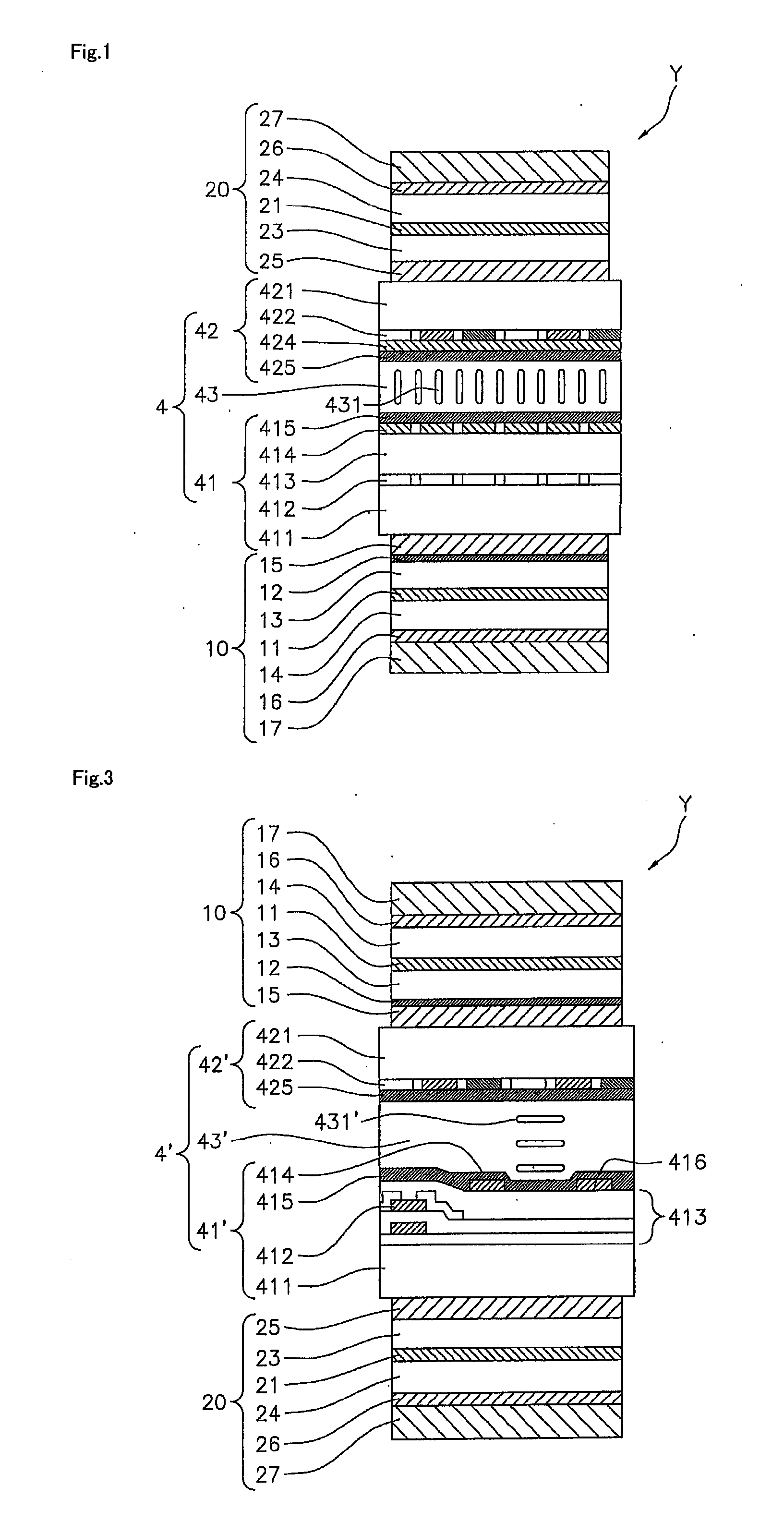
[0061]FIG. 1 shows a schematic cross-sectional view of a liquid crystal display panel Y. The liquid crystal display panel Y includes a rectangular liquid crystal cell 4 including a liquid crystal layer 43 placed between a pair of first and second substrates 41 and 42; a first polarizing plate 10 placed on the first substrate 41 side of the liquid crystal cell 4; and a second polarizing plate 20 placed on the second substrate 42 side of the liquid crystal cell 4.

[0062]Liquid Crystal Cell

[0063]In this embodiment, a vertical alignment-type (hereinafter referred to as “VA-type”) liquid crystal cell is used as the liquid crystal cell 4. The VA-type liquid crystal cell 4 is described below.

[0064]The first substrate 41 (hereinafter also referred to as the backside substrate) placed on the backside (backlight side) of the liquid crystal cell 4 includes a transparent substrate 411 of glass, plastic or the like; a circuit part that is provided on the transparent substrate 411 and includes a p...

embodiment 2

[0135]A description is given of a case where an in-plane switching (IPS)-type liquid crystal cell is used.

[0136]FIG. 3 is a schematic cross-sectional view of a liquid crystal display panel Y with an IPS-type liquid crystal cell.

[0137]In FIG. 4, the same elements are represented by the same reference characters as in FIG. 1, and a repeated description thereof will be omitted as appropriate. As shown in FIG. 4, an IPS-type liquid crystal cell 4′ is configured to have a liquid crystal layer 43′ placed between a pair of substrates 41′ and 42′ similarly to other liquid crystal cells. The display surface side substrate 42′ located on the display surface side of the liquid crystal cell 4′ does not have any electrically-conductive components such as pixel electrodes and a common electrode. In contrast, the backside substrate 41′ located on the back side of the liquid crystal cell 4′ is configured to have a common electrode and pixel electrodes for driving the liquid crystal layer 43′, so th...

example 1

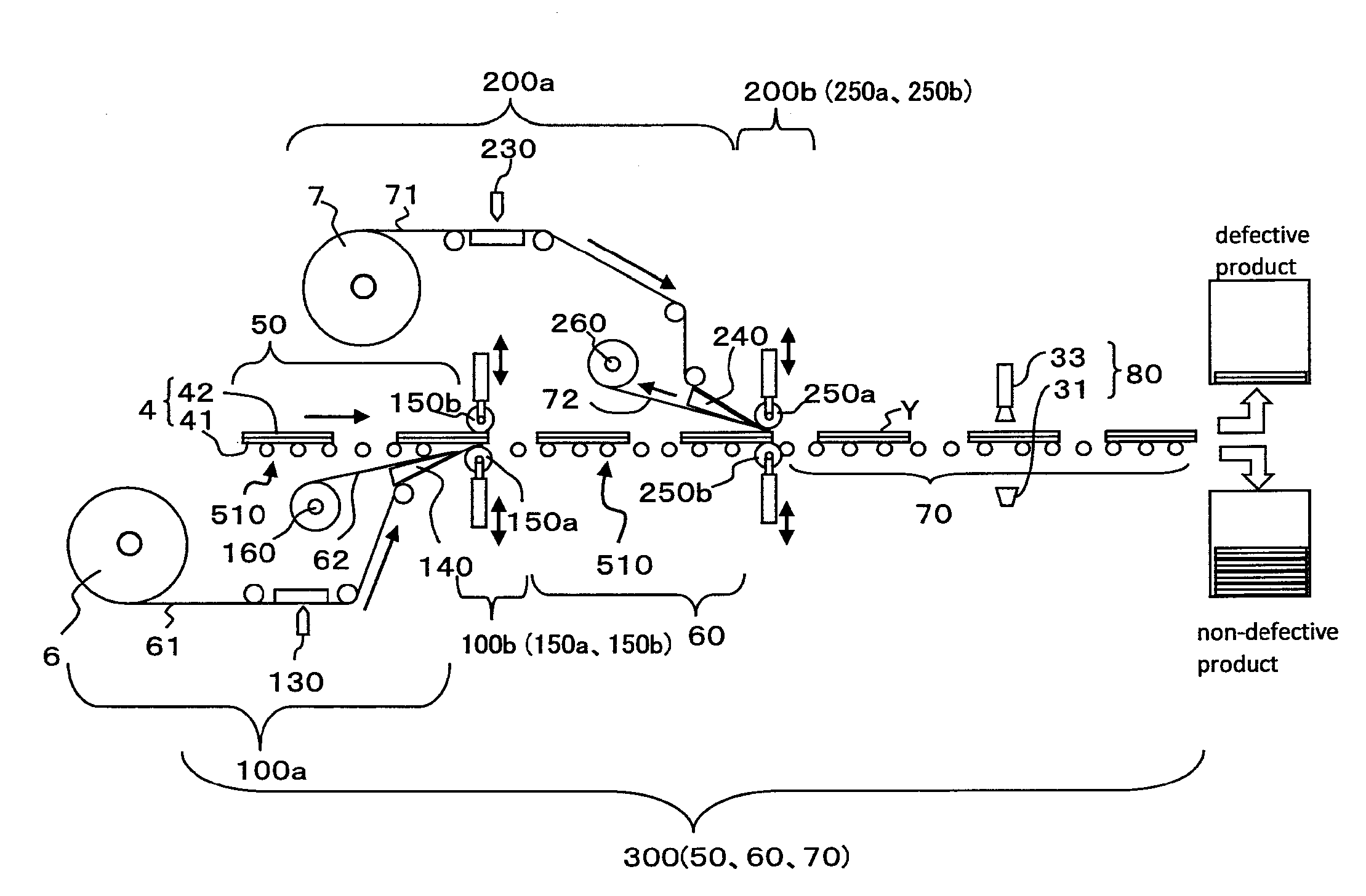
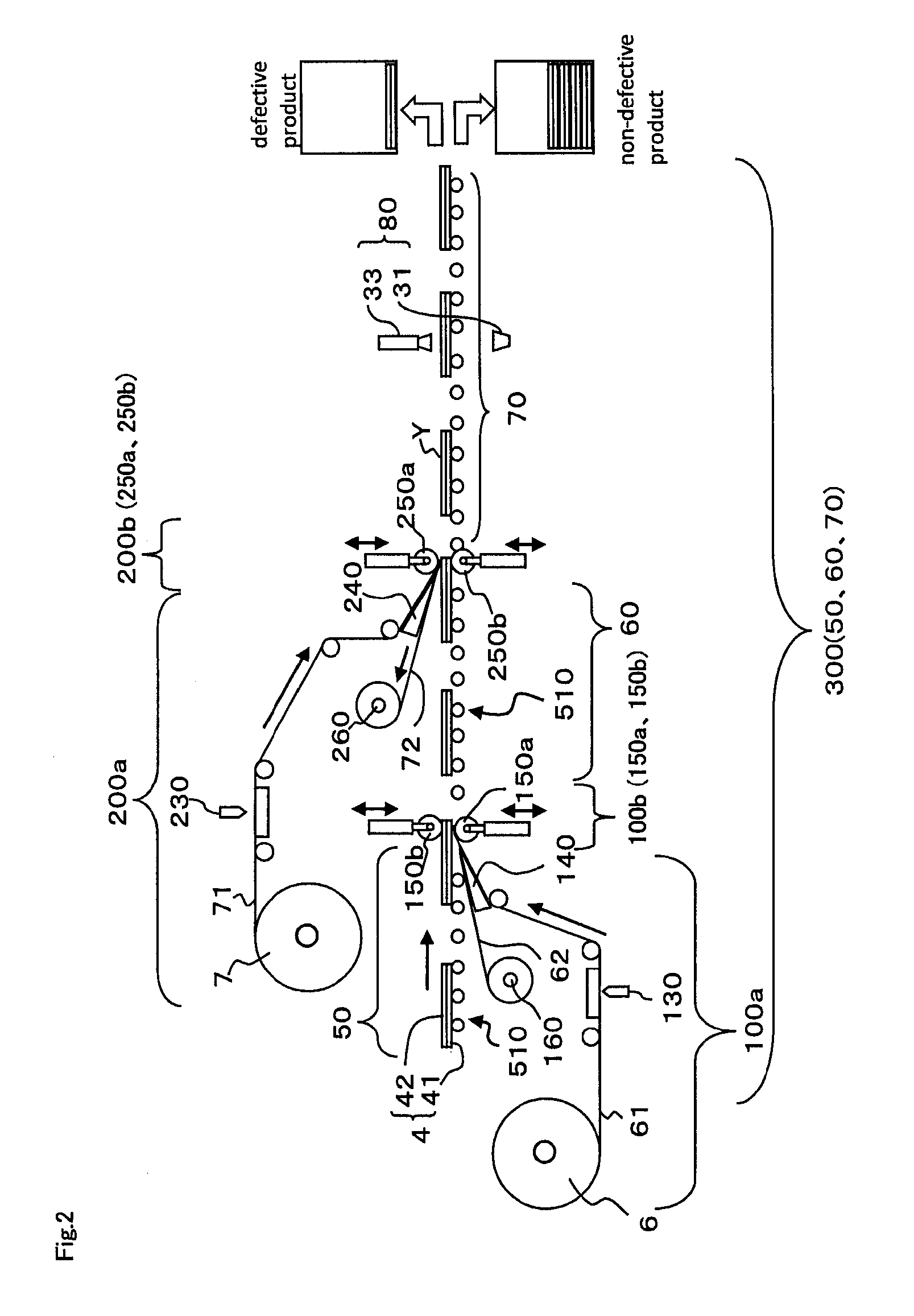
[0152]The continuous manufacturing system shown in FIG. 2 was used. A first polarizing plate with a width corresponding to the long side of the VA-type liquid crystal cell was bonded to the liquid crystal cell (the first polarizing plate bonding step), and then the liquid crystal cell was horizontally turned by 90° and aligned. Subsequently, a second polarizing plate with a width corresponding to the short side of the liquid crystal cell was bonded to the liquid crystal cell (the second polarizing plate bonding step). In this manner, 2,000 liquid crystal display panels were continuously manufactured. The speed at which each polarizing plate was bonded and the speed at which the liquid crystal cell and the liquid crystal display panel were fed were 200 mm / second. The materials and apparatuses used were as described below. The surface resistance of the electrically-conductive layer contained as a part in the polarizing plate was measured according to JIS K 6911, 5.13. Specifically, th...


PUM

PropertyMeasurementUnit
thicknessaaaaaaaaaa
thicknessaaaaaaaaaa
thicknessaaaaaaaaaa

Abstract

The invention is a method for continuously manufacturing an inspected liquid crystal display panel, includes: a liquid crystal cell feeding step including feeding a liquid crystal cell having a first substrate and a second substrate; a first polarizing plate providing step including providing a first polarizing plate from a first polarizing plate roll; a first polarizing plate laminating step including laminating the first polarizing plate to the first substrate; a second polarizing plate providing step including providing a second polarizing plate from a second polarizing plate roll; a second polarizing plate laminating step including laminating the second polarizing plate to the second substrate to obtain a liquid crystal display panel after laminating the first polarizing plate to the first substrate; and an inspecting step including optically inspecting the liquid crystal display panel without applying voltage to the liquid crystal panel, wherein the first substrate is less susceptible to electrostatic decay in the liquid crystal cell than the second substrate.

Description

BACKGROUND OF THE INVENTION[0001]1. Field of the Invention[0002]The invention relates a system and a method for continuously manufacturing liquid crystal display panels. More specifically, the invention relates to a system and a method for manufacturing liquid crystal display panels by a process that includes sequentially bonding first and second polarizing plates, which are drawn and supplied from first and second polarizing plate rolls, respectively, to both surfaces of a liquid crystal cell to form a liquid crystal display panel; and optically inspecting the liquid crystal display panel.[0003]2. Background Art[0004]A system for continuously manufacturing liquid crystal display panels is disclosed, in which first and second polarizing plates, which are drawn and supplied from first and second polarizing plate rolls, respectively, are sequentially bonded to both surfaces of a liquid crystal cell to form a liquid crystal display panel (Japanese Patent Application Laid-Open (JP-A) No...

Claims


Application Information

Patent Timeline
Patent Type & Authority Applications(United States)
IPC IPC(8): B29C65/42
CPCG02F1/1309G02F1/1333G02F2202/28G02F2202/22G02F1/133528G02F1/13G02F1/1335
Inventor KOSHIO, SATORUKITADA, KAZUOYURA, TOMOKAZUNAKAZONO, TAKUYATAKIGAWA, MASAHIRO
Owner NITTO DENKO CORP
Why Eureka
Try Eureka