Current-Based Method and Apparatus for Detecting and Classifying Arcs

a current-based, arc-detecting technology, applied in the direction of resistance/reactance/impedence, material breakdown voltage, instruments, etc., can solve the problem of unintended low impedance path from the anode to the target, unintended low impedance path, yield-reducing defects in forming integrated circuits on semiconductor wafers, etc. problem, to achieve the effect of reducing the power supply response to the arc, reducing defects, and improving the yield of wafer

Active Publication Date: 2008-01-24
SCHNEIDER ELECTRIC USA INC
View PDF5 Cites 40 Cited by
  • Summary
  • Abstract
  • Description
  • Claims
  • Application Information

AI Technical Summary

Benefits of technology

[0025] Actual micro-arcs (e.g., as captured on an oscilloscope) show a rapid decrease (followed by a recovery to a nominal value) in voltage magnitude and simultaneously, a rapid increase (also followed by a recovery to a nominal value) in current magnitude. Accordingly, looking at the current level for spikes, and looking at the voltage level for simultaneous decreases greatly increase the confidence level or success rate of “true” arc detection. The present invention provides embodiments of a method and apparatus for detecting such arc events, and for detecting and classifying other arc events.
[0036] The method further includes delaying comparing the voltage to the voltage threshold value and the current to the current threshold value for a transition delay period after each detection of an arc event. This provides a more accurate arc event count for the stable mode.
[0050] The present invention enhances the ability to determine in real-time when arcing is occurring so that corrective action may be taken. This can improve wafer yield and reduce defects.

Problems solved by technology

However, uniformity of electric field cannot be maintained perfectly and the uniformity of the glow discharge and henceforth wear on the target is influenced by a number of factors, including thermal currents generated in the chamber and other mechanical anomalies, such as target misalignment.
Even with the rotating magnet mechanism in place to attempt to stabilize the glow discharge, certain conditions can result in a local concentration of the electric field causing the glow discharge to pass from the superconducting region of the Paschen curve into the arcing region.
Arcing during PVD results in an unintended low impedance path from the anode to the target through electrons or ions in the plasma, the unintended path generally including ground, with the arcing being caused by factors such as contamination (i.e., inclusions) of the target material, inclusions within the structure (e.g., surface) of the target, improper target alignment (e.g., misalignment of cathode and anode), vacuum leaks, and / or contamination from other sources such as vacuum grease.
Arcing during PVD is one cause of yield-reducing defects in forming integrated circuits on semiconductor wafers.
The dislodged solid piece of target material may be large relative to the thickness of the uniform coating expected on the wafer, and if a large piece falls upon the wafer, it may cause a defect in the integrated circuit being formed at that location.
Because arcing results in a localized defect (area) having a greater thickness than the surrounding metal, the defect area may not be thoroughly etched in the subsequent processing, resulting in an unintended circuit path (i.e., short) on the chip.
A local defect in one layer can also distort an overlying pattern imaged onto the wafer in a subsequent photolithography step, and thus result in a defect in an overlying layer.
Arcing in a PVD sputtering apparatus used to process wafers into integrated circuits can render portions of the wafer useless for its intended purpose, thereby increasing manufacturing costs.
Using target materials free of arc-causing inclusions is one way of minimizing integrated circuit fabrication defects; however, target material may become contaminated during its manufacture or thereafter.
Discovering target contamination prior to sputtering operations so as to prevent arcing defects is costly, both in terms of time and expense.
Not discovering arcing defects in a timely manner is similarly costly in terms of random yield loss, for example by the manufacturer operating a deposition chamber until the target inclusion causing the arcing is sputtered through.
Furthermore, when a solid piece of the target is dislodged during an arc, the surface of the target may be further damaged and the potential for future arcing in that neighborhood increases.
It is costly to measure the number of defective layers caused by arcing, for example via electrical tests designed to reveal shorts or by scanning the surface of wafers with a laser after metal deposition.
These tests take time to run, during which production is delayed, or undetected yield loss occurs for an extended time.
As discussed above, arcs can throw solid material into the chamber, and it can be assumed that any such piece of solid material landing on a wafer of integrated circuits has a high probability of damaging at least one integrated circuit.
When this occurs, the presence of series inductance in the driving point impedance of the power delivery system, comprising power supply and interconnection means, causes a rapid drop in the magnitude of observed voltage between the anode and cathode of the chamber.
As such, such a system may miss arcs of small magnitude, which nonetheless cause damage.
Electronically controlled analog or switching power supplies cannot react to this rapid change in chamber impedance during a microarc.
While useful for gaining an understanding of the arcing phenomenon in PVD applications, this method of computing arcs and arc energy using an oscilloscope and a post processing computer is of little value in production applications.
Even modem handheld oscilloscopes are relatively bulky instruments, and real estate in an integrated circuit clean room is extremely valuable.
A stand alone post processing computer also takes up valuable floor space and would likely need to be located outside the clean room and connected to the oscilloscope by a network, adding latency in the transfer of data between the oscilloscope and computer.
Furthermore, there is no means to tell a-priori the duration of an individual arc, or the frequency at which they might occur, leaving the problem of exactly how to set the controls of the oscilloscope.
Oscilloscopes also have limited waveform storage capability, and therefore prone to losing information at the times in which it is needed most, when there is much arcing activity during a process.
A system so configured would render real time control and decision making impractical.
In addition to the problems discussed, when counting arcs only as voltage threshold violations, some information may be lost or obscured if the power supply responds to the arcs by reducing delivered power.
The result of reducing power is a dip in both the voltage and the current.

Method used


Image

  • Current-Based Method and Apparatus for Detecting and Classifying Arcs
  • Current-Based Method and Apparatus for Detecting and Classifying Arcs
  • Current-Based Method and Apparatus for Detecting and Classifying Arcs

Examples


Embodiment Construction

[0081] While this invention is susceptible of embodiments in many different forms, there is shown in the drawings and will herein be described in detail preferred embodiments of the invention with the understanding that the present disclosure is to be considered as an exemplification of the principles of the invention and is not intended to limit the broad aspect of the invention to the embodiments illustrated.

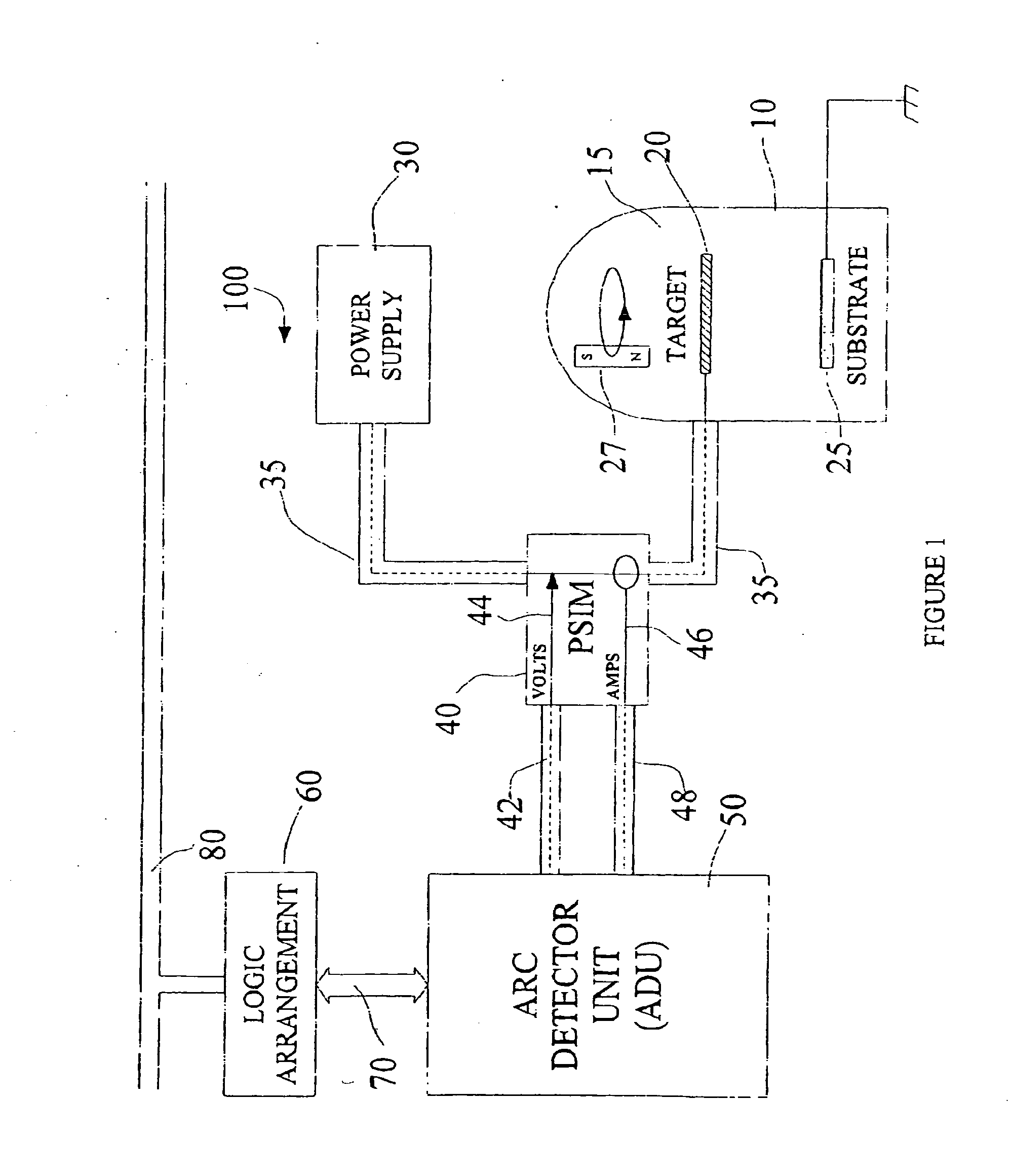
[0082] The present invention is believed to be applicable to a variety of different types of plasma generation applications, and has been found to be particularly useful for film deposition applications, the latter benefiting from a technique for responding to detected arcs during the generation of a plasma environment. Example embodiments described herein involve PVD sputtering techniques; however, the present invention can be implemented in connection with a variety of systems, including those using plasma-generating techniques such as plasma etching or Plasma Enhanced Chem...


PUM

PropertyMeasurementUnit
thickaaaaaaaaaa
voltageaaaaaaaaaa
currentaaaaaaaaaa

Abstract

An apparatus and technique are provided for generating a plasma using a power supply circuit and arc detection arrangement. The power supply circuit has a cathode enclosed in a chamber, and is adapted to generate a power-related parameter. The arc detection arrangement is communicatively coupled to the power supply circuit and adapted to assess the severity of arcing in the chamber by comparing the power-related parameter to at least one threshold. According to various implementations, arc occurrences, arcing duration, intensity and / or energy are measured responsive to comparing the power-related parameter to the at least one threshold. According to further implementations, the above-mentioned measured quantities are accumulated and / or further processed. An apparatus and method are also provided for detecting arc events when the current spikes above a threshold level. The method and apparatus is also for classifying the arc events based on the voltage and current signals and the duration each is beyond a threshold value.

Description

CROSS-REFERENCE TO RELATED APPLICATIONS [0001] The present invention is a continuation-in-part of U.S. patent application Ser. No. 10 / 769,023, filed Jan. 30, 2004, which is a continuation of U.S. patent application Ser. No. 10 / 121,445, filed Apr. 12, 2002. The present invention also claims the benefit of priority of U.S. Provisional Patent Application No. 60 / 783,346 for “Current-Based Method and Apparatus for Detecting and Classifying Arcs” filed Mar. 17, 2006.TECHNICAL FIELD [0002] The invention generally relates to a method and apparatus for detecting and classifying arcs in a device, and more particularly, to a method and apparatus for detecting and classifying arcs in a physical vapor deposition process by examining the current and voltage, and timing the duration each goes beyond one or more threshold values. BACKGROUND OF THE INVENTION [0003] Sputtering deposition, such as Physical Vapor Deposition (PVD), is a process for depositing thin, highly uniform layers of a variety of ...

Claims


Application Information

Patent Timeline
Patent Type & Authority Applications(United States)
IPC IPC(8): G01N27/92G01R25/08
CPCG01R19/0061H01J2237/0206H01J37/32935
Inventor KRAUSS, ALAN F.HARRIS, RAYMOND W.BUDA, PAUL R.
Owner SCHNEIDER ELECTRIC USA INC
Why Eureka
Try Eureka