Thin Group IV Semiconductor Structures
- Summary
- Abstract
- Description
- Claims
- Application Information
AI Technical Summary
Benefits of technology
Problems solved by technology
Method used
Image

Examples
example 1
Ge / Si(100) Structures and Templates
[0065]Pure Ge films directly on Si substrates with unprecedented control of film microstructure, morphology, purity and optical properties can be grown via CVD (see, Wistey, supra; and Fang supra). Ge growth is conducted at low temperatures (about 350° C. to about 420° C.) on a single wafer reactor configuration at about 10−5 to about 10−4 Torr, in the absence of gas phase reactions using molecular mixtures of Ge2H6 and small amounts of highly reactive (GeH3)2CH2 or GeH3CH3 organometallic additives.
[0066]The optimized molar ratios of these compounds have enabled layer-by-layer growth at conditions compatible with selective growth, which has recently been demonstrated by depositing patterned Ge “source / drain” structures in prototype devices. The driving force for this reaction mechanism is the facile elimination of extremely stable CH4 and H2 byproducts, consistent with calculated chemisorption energies and surface reactivities.
[0067]Using this appr...
example 2
Doped Ge / Si(100)
[0071]The n-type doping of the Ge layers grown directly on Si can be conducted using proven protocols that have already led to the successful doping of the Ge1-xSnx alloys. These utilize As, Sb, P custom prepared hydride compounds such as As(GeH3)3, P(GeH3)3 and Sb(GeH3)3 molecules. These are co-deposited with mixtures of digermane to form Ge films incorporating the appropriate carrier type and level. In the case of As, we have been able to introduce free carrier concentrations as high as 1020 / cm3 in Ge1-xSnx via deposition of As(GeH3)3. These carbon-free hydrides are ideal for low temperature, high efficiency doping applications. They are designed to furnish a structural Ge3As unit resulting inhomogeneous substitution at high concentrations without clustering or segregation. For p-type doping suitable concentrations of gaseous B2H6 can be mixed with the Ge precursors and reacted to obtain the desired doping level.
[0072]In one example, p-type Ge layers with thickness...
example 3
Optoelectronic Ge1-ySny Alloys
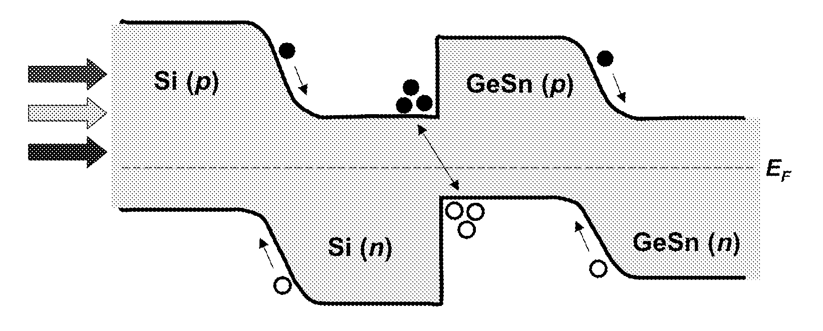
[0075]From a fundamental view point Ge1-ySny alloys on their own right are intriguing IR materials that undergo an indirect-to-direct band gap transition with variation of their strain state and / or compositions. They also serve as versatile, compliant buffers for the growth of II-VI and III-V compounds on Si substrates.
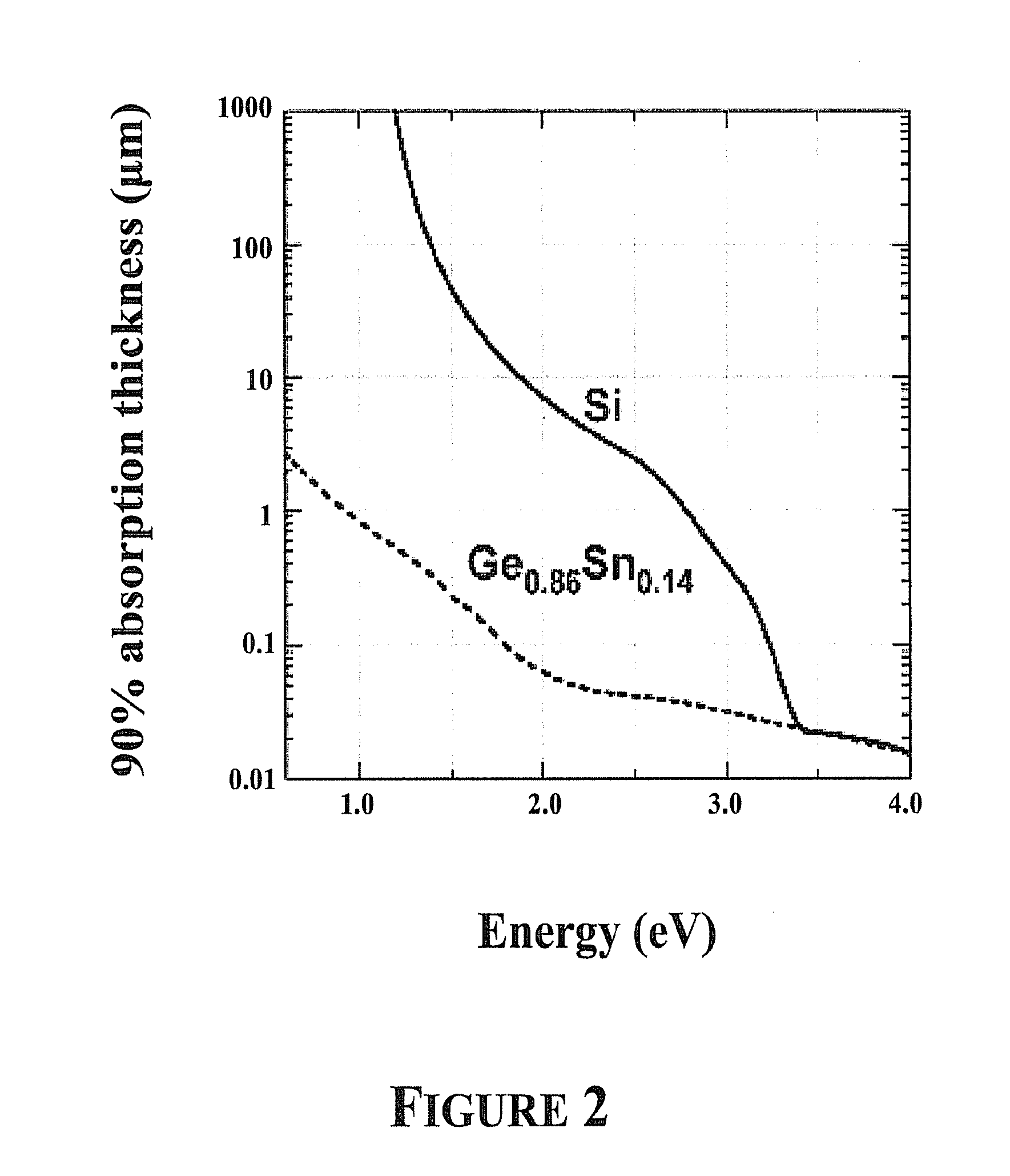
[0076]The fabrication of the Ge1-ySny materials directly on Si wafers has recently been reported using a specially developed CVD method involving reactions of Ge2H6 with SnD4 in high purity H2 (10%). Thick and atomically flat films are grown at about 250° C. to about 350° C. and possess low densities of threading dislocations (about 105 cm−2) and high concentrations of Sn atoms up to about 20%. Since the incorporation of Sn lowers the absorption edges of Ge, the Ge1-ySny alloys are attractive for photovoltaic applications that require band gaps lower than that of Ge (0.80 eV). The absorption coefficient of selected Ge1-xSnx samples, showi...
PUM
 Abstract
Description
Claims
Application Information
 - Generate Ideas
- Intellectual Property
- Life Sciences
- Materials
- Tech Scout
- Unparalleled Data Quality
- Higher Quality Content
- 60% Fewer Hallucinations
Browse by: Latest US Patents, China's latest patents, Technical Efficacy Thesaurus, Application Domain, Technology Topic, Popular Technical Reports.
© 2025 PatSnap. All rights reserved.Legal|Privacy policy|Modern Slavery Act Transparency Statement|Sitemap|About US| Contact US: help@patsnap.com