Method for forming sapphire substrate and semiconductor device

Active Publication Date: 2012-01-12
YAMAGUCHI UNIV
View PDF4 Cites 30 Cited by
  • Summary
  • Abstract
  • Description
  • Claims
  • Application Information

AI Technical Summary

Benefits of technology

[0020]A plurality of tapered projections can be arranged at random on a sapphire substrate through a small number of process steps at low cost. The use of this substrate enables fabrication of a light-emitting diode exhibiting a high light-extraction efficiency.

Problems solved by technology

In the GaN layer grown on the sapphire substrate, however, threading dislocation serving as a high-density nonradiative recombination center occurs in GaN crystal because of lattice mismatch between a sapphire crystal lattice and a GaN crystal lattice.
That is, total internal reflection due to the difference in refractive index greatly reduces the light-extraction efficiency of an LED.

Method used


Image

  • Method for forming sapphire substrate and semiconductor device
  • Method for forming sapphire substrate and semiconductor device
  • Method for forming sapphire substrate and semiconductor device

Examples


first embodiment

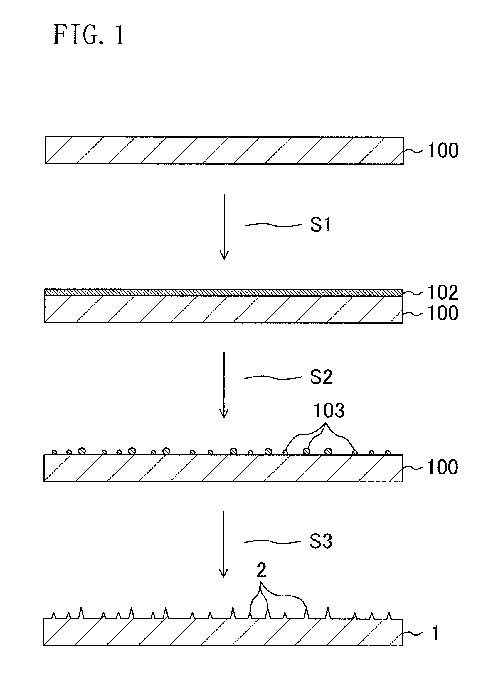
[0033]A method for forming a sapphire substrate 1 according to a first embodiment will be described based on a flow of formation schematically shown in FIG. 1.

[0034]A disc-shaped thin sapphire plate 100 made of single crystal with a corundum structure of Al2O3is prepared. The thin sapphire plate 100 has a diameter of 50 mm to 300 mm, and a thickness of 0.3 mm to 3 mm. The thin sapphire plate 100 can be formed at a cost much lower than a thin GaN plate, and is much superior to a thin Si plate in device performance in view of light transmittance. In addition, a surface (i.e., a principal surface) of the thin sapphire plate 100 on which a GaN layer is to be formed in formation of a compound semiconductor, which will be described later, may be an a plane , a c plane , an m plane , or an r plane , or may be a crystal plane of another plane orientation.

[0035]

[0036]A metal is deposited by evaporation on a surface (i.e., the principal surface) of the thin sapphire plate 100, thereby forming...

second embodiment

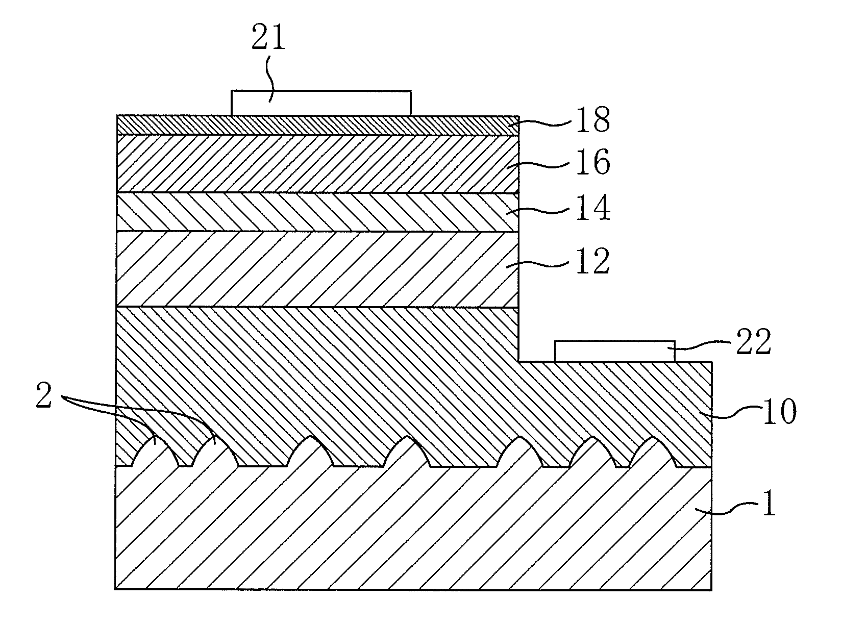
[0058]A second embodiment of the present disclosure differs from the first embodiment in a thin sapphire plate, and the other part of the configuration is the same as in the first embodiment. Thus, aspects different from those in the first embodiment will be described hereinafter. FIG. 11 shows a sapphire substrate 1′ of this embodiment.

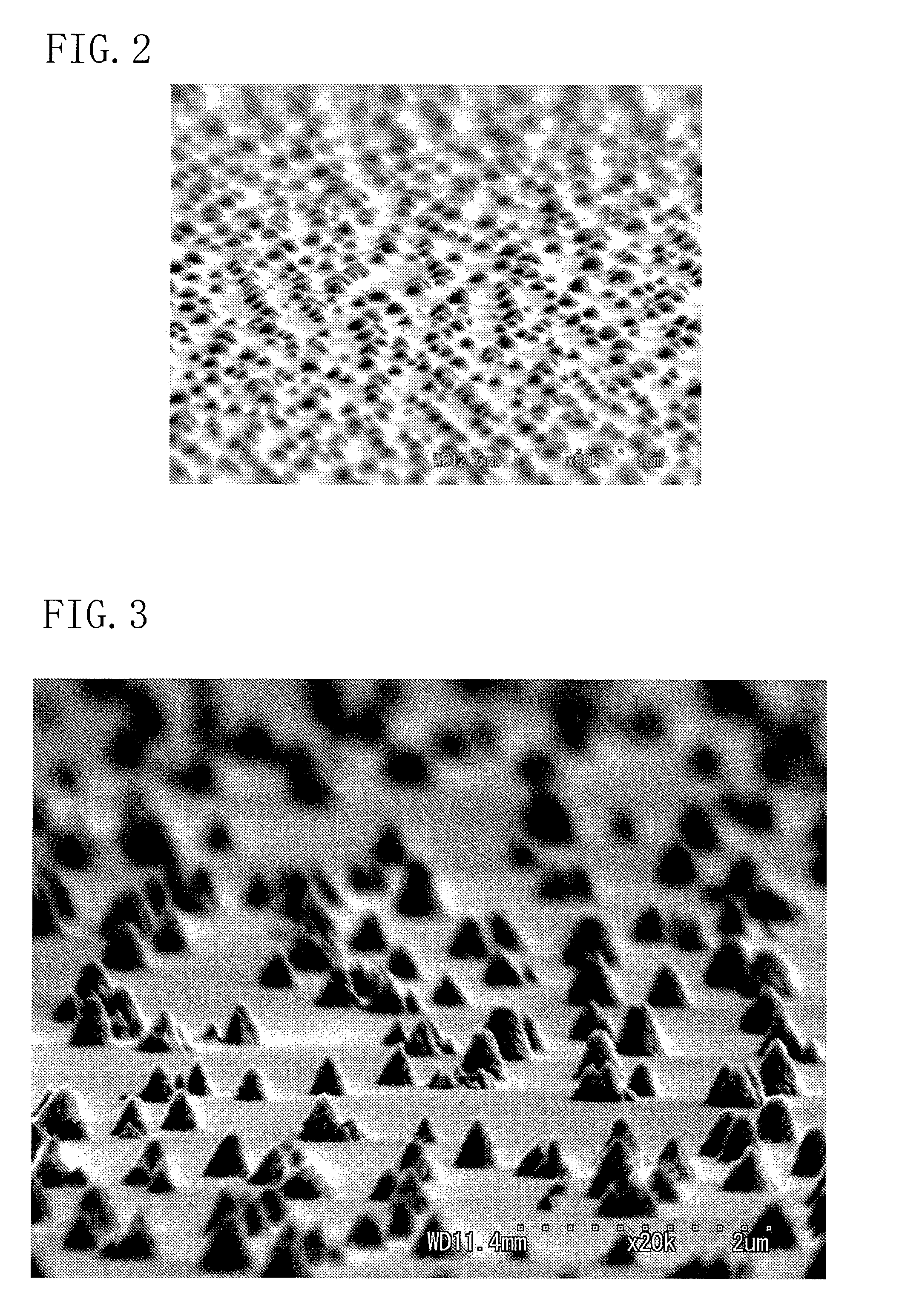
[0059]In the thin sapphire plate of this embodiment, a plurality of convex shapes 2′ are previously arranged at random on a principal surface 3. Each of the convex shapes 2′ is tapered from the bottom to the top thereof. The density of the convex shapes 2′ is in the range from 1×10⁵ / cm2to 5×10⁷ / cm2, both inclusive. The area of a flat portion of the top 4′ of each of the convex shapes 2′ is larger than 0 (zero) and smaller than or equal to 10 μm2. The bottom surface of each of the convex shapes 2′ has a longer diameter of 1 μm to 50 both inclusive, and a shorter diameter of 100 nm to 10 μm, both inclusive. Using this thin sapphire plate, a sapphire su...


PUM

PropertyMeasurementUnit
Lengthaaaaaaaaaa
Lengthaaaaaaaaaa
Thicknessaaaaaaaaaa

Abstract

In a semiconductor device fabricated by growing a compound semiconductor layer on a sapphire substrate, a sapphire substrate enabling the semiconductor device to have a high light-extraction efficiency is provided.A plurality of projections 2, 2, . . . are provided at random on a surface of a sapphire substrate 1, and a GaN layer 10 is grown on this surface. Then, a multi-quantum well layer 12, a p-AlGaN layer 14, a p-GaN layer 16, and an ITO layer 18 are formed on the GaN layer 10, and two electrodes 21 and 22 are also formed. In this manner, a semiconductor light-emitting device is fabricated.

Description

TECHNICAL FIELD[0001]The present disclosure relates to methods for forming sapphire substrates and semiconductor devices.BACKGROUND ART[0002]Light-emitting diodes (LEDs) are often used for various types of lighting devices, illumination, electronic equipment, and the like, for their high energy conversion efficiencies and long lives. An LED capable of emitting visible light is generally fabricated using AlGaInN (hereinafter typified by GaN) or a Group III-V compound semiconductor material of AlGaInP GaN is used for LEDs which emit green light, blue light, or ultraviolet light. AlGaInP is used for LEDs which emit red light, orange light, or yellow light.[0003]At present, GaN crystal is grown on a sapphire (Al2O3) substrate in consideration of, for example, cost and quality. In the GaN layer grown on the sapphire substrate, however, threading dislocation serving as a high-density nonradiative recombination center occurs in GaN crystal because of lattice mismatch between a sapphire cry...

Claims


Application Information

Patent Timeline
IPC IPC(8): H01L21/20
CPCC30B25/18C30B29/403C30B29/406H01L33/007H01L21/0243H01L21/0254H01L21/02658H01L21/0242C23C14/14C23C14/58C30B33/12H01L21/3065H01L33/00
Inventor TADATOMO, KAZUYUKIOKADA, NARIHITO
Owner YAMAGUCHI UNIV
Why Eureka
Try Eureka