Method and device for preparing compound semiconductor film

a semiconductor film and compound technology, applied in the field of solar batteries, can solve the problems of poor coating material distribution, poor solar battery life, and low preparation area of battery area less than 1 cm

Inactive Publication Date: 2012-01-19
BYD CO LTD
View PDF3 Cites 6 Cited by
  • Summary
  • Abstract
  • Description
  • Claims
  • Application Information

AI Technical Summary

Benefits of technology

[0007]In viewing thereof, the present invention is directed to solve at least one of the problems existing in the prior art. Accordingly, a method for prepar...

Problems solved by technology

Therefore, this kind of solar batteries may have a long lifespan.
However, the battery area prepared is far less than 1 cm2, which is mainly limited by emitting characteristics of the evaporation source.
While preparing thin film with a large area, the coating material distribution is severely uneven.
The larger the scale is, the more uneven the material distribution is.
Due to the large area requirement to the solar battery, this method does not have industrial commercialbility.
Although semiconductor film with relatively large area may be achieved in this case, the un...

Method used


Image

  • Method and device for preparing compound semiconductor film
  • Method and device for preparing compound semiconductor film
  • Method and device for preparing compound semiconductor film

Examples


first embodiment

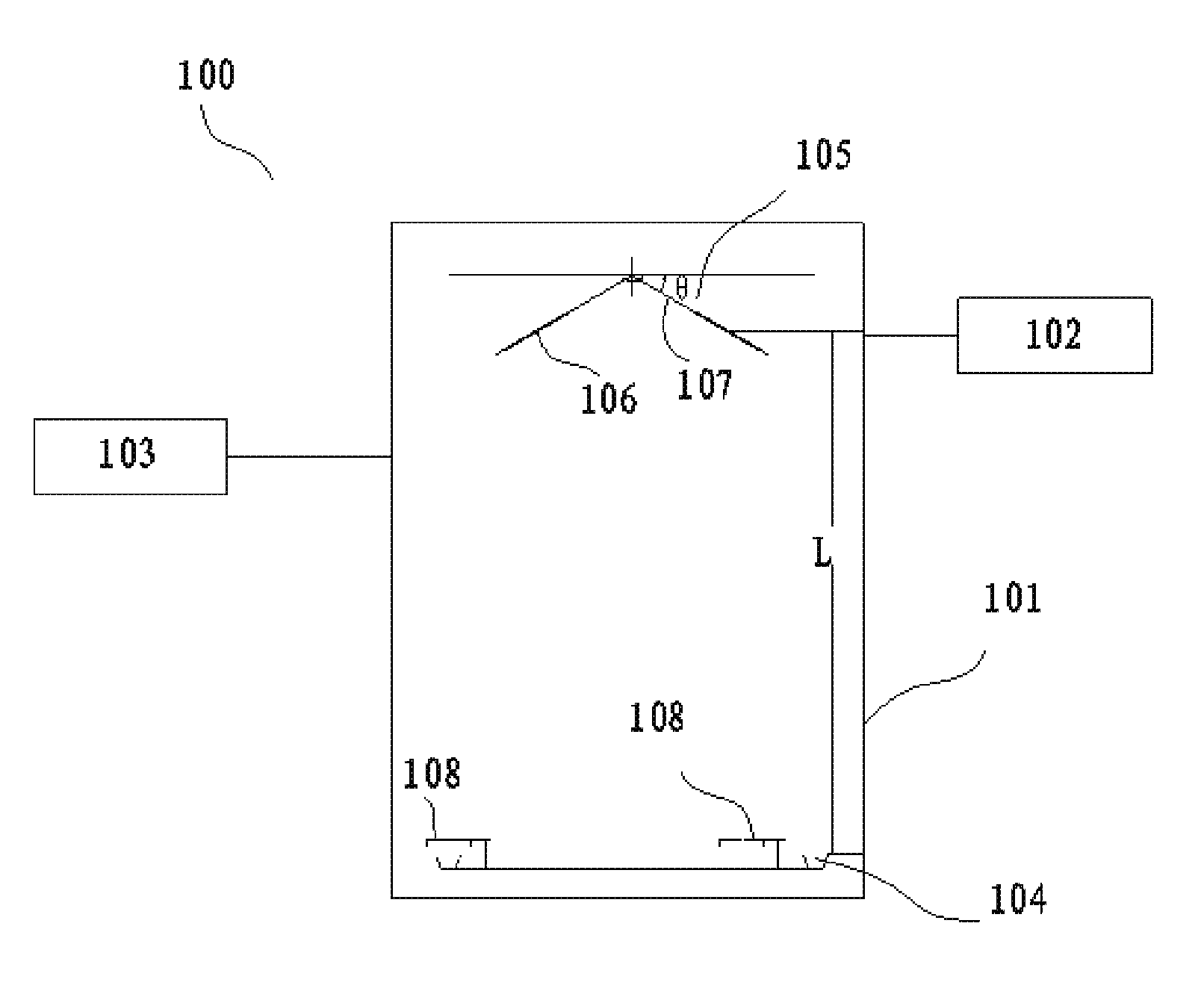
[0048](1) The substrate after ultrasonic cleaning is fixed by, for example, a substrate clamp and the angle between the substrate and the plane is 8 degrees. The substrate has an area of 15×15 cm2 and it is a NaCa glass which is magnetron sputtered by a layer of Mo electrode substrate having a thickness of 1 μm.

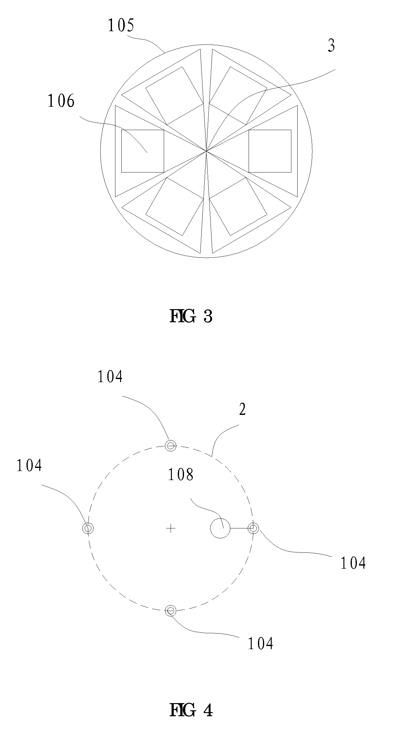
[0049](2) Evaporation sources with Cu, In, Ga and Se are uniformly fixed in a phantom circle at the four quartering points respectively. The circle has a radius of 9 times of the side length of the substrate.

[0050](3) Then, it is vacuumized by the vacuumizing unit 102 to 3.0×10⁻³ Pa and the device 100 for implementing the method of the invention is heated to further remove gas contained herein until the vacuum degree reaches up to 2.0×10⁻⁴ Pa. Meanwhile the substrate is heated up to 500° C., then the temperature is maintained thereafter.

[0051](4) The evaporation speed of each evaporation source may be adjusted. The evaporation speed of the Cu evaporation source is about 15 nm...

second embodiment

[0054]Compared with First Embodiment, the only difference may lie in that the angle between the substrate and the plane is 5 degree. The radius of the circle is about 8 times of the side length of the substrate. And the rotating speed of the substrate is about 20 rad / min, the remaining features thereof is the same as First Embodiment, and the substrate may be denominated as A2.

third embodiment

[0055]Compared with First Embodiment, the only difference may lie in that the angle between the substrate and the plane is 30 degree. The radius of the circle is ten times of the side length of the substrate. The rotating speed of the substrate is about 90 rad / min, the remaining features are the same as First Embodiment, and the substrate may be denominated as A3.


PUM

PropertyMeasurementUnit
Temperatureaaaaaaaaaa
Angleaaaaaaaaaa
Angleaaaaaaaaaa

Abstract

The present invention discloses a method and a device for preparing a compound semiconductor film. The method comprises the steps of: providing a substrate above at least an evaporation source in a vacuum condition; heating a source material contained in the evaporation source so that the source material is vapor-deposited on the substrate; and taking out the substrate under protection of an inert gas. The substrate may be rotated around an axis of a plane where the evaporation source is positioned, and the substrate is tilted by a predetermined angle with respect to the plane. The compound semi-conductive film thus prepared has a uniform thickness with a larger area. The method provides a simplified process and enhanced efficiency.

Description

CROSS REFERENCE RELATED APPLICATION[0001]This application claims priority to Chinese Patent Application No. 200910106258.9, filed to SIPO on Mar. 31, 2009, the entirety of which is hereby incorporated by reference.TECHNICAL FIELD 0F THE INVENTION[0002]The present invention relates to the field of solar battery, more particularly to a method and a device for preparing a compound semiconductor film respectively.BACKGROUND 0F THE INVENTION[0003]Solar batteries of compounded semiconductor film series are one of the most efficient and potential ones in thin-film solar batteries. Compound semiconductor material has the highest light absorption coefficient in known semiconductor materials, which may reach up to 105 / cm, without semiconductors having S-W effect (Staebler-Wronski Effect). Moreover, converting efficiency thereof may be enhanced by light irradiation. Therefore, this kind of solar batteries may have a long lifespan. It is shown by experiments that compound semiconductor film sol...

Claims


Application Information

Patent Timeline
IPC IPC(8): H01L21/20C23C16/458C23C16/455
CPCC23C14/0623Y02E10/543C23C14/24H01L21/02568H01L21/02631H01L31/04H01L31/18C23C14/505H01L21/02422H01L21/02491H01L31/03923H01L31/03925H01L31/1828H01L31/0322Y02E10/541C23C14/225
Inventor ZHONG, BEIJUNCAO, WENYUZHOU, YONGJIANG, ZHANFENG
Owner BYD CO LTD
Why Eureka
Try Eureka