Two terminal resistive switching device structure and method of fabricating

a switching device and resistive technology, applied in the direction of semiconductor/solid-state device manufacturing, basic electric elements, electric devices, etc., can solve the problems of increasing power dissipation, preventing proper device operation, and non-scaling of sub-threshold slopes

Active Publication Date: 2012-01-19
CROSSBAR INC
View PDF13 Cites 103 Cited by
  • Summary
  • Abstract
  • Description
  • Claims
  • Application Information

AI Technical Summary

Benefits of technology

[0009]In a specific embodiment, a method for forming a two terminal switching device is provided. The method includes providing a substrate and forming a first dielectric material overlying a surface region of the substrate. A bottom wiring material is deposited overlying the dielectric material. The method includes depositing a contact material overlying the bottom wiring material and depositing a switching material overlying the bottom wiring material; including the contact material. In certain embodiment, the contact material is optional. The method forms a masking layer overlying the switching material. In a specific embodiment, the method subjects the bottom wiring material, the contact material,-and the switching material to a first etching process using the masking layer to form a first structure. The first structure includes a bottom wiring structure and a switching element. The first structure has a top surface region and a side region. In a specific embodiment, the top surface region including a top region of the switching element. The method includes depositing a second dielectric material overlying at least the first structure including the exposed top region of the switching element and an exposed portion of the first dielectric material. The method includes planarizing the second dielectric material surface overlying at least the first structure while maintaining a portion of the second dielectric material overlying the first structure. An opening region is formed in a portion of the second dielectric layer to expose a portion of the top surface region of the first structure. The method then deposits a conductive material overlying the opening region. The conductive material is in direct contact with the switching element in a specific embodiment. A top wiring material is formed overlying at least the conductive material, and a second etching process is employed to form at least a top wiring structure. In a specific embodiment, the side region of the first structure including a first side region of the switching element is free from a contaminant conductive material from the second etching process.
[0010]In an alternative embodiment, a method for forming a two terminal switching device is provided. The method includes providing a substrate and forming a first dielectric material overlying a surface region of the substrate. A bottom wiring material is deposited overlying the dielectric material. The method includes depositing a contact material ...

Problems solved by technology

However, as field effect transistors (FET) approach sizes less than 100 nm, problems such as short channel effect start to prevent proper device operation.
Moreover, such sub 100 nm device size can lead to sub-threshold slope non-scaling and also increases power dissipation.
These devices often require new materials and device structures to couple with silicon based devices to form a memory cell, which lack ...

Method used


Image

  • Two terminal resistive switching device structure and method of fabricating
  • Two terminal resistive switching device structure and method of fabricating
  • Two terminal resistive switching device structure and method of fabricating

Examples


Embodiment Construction

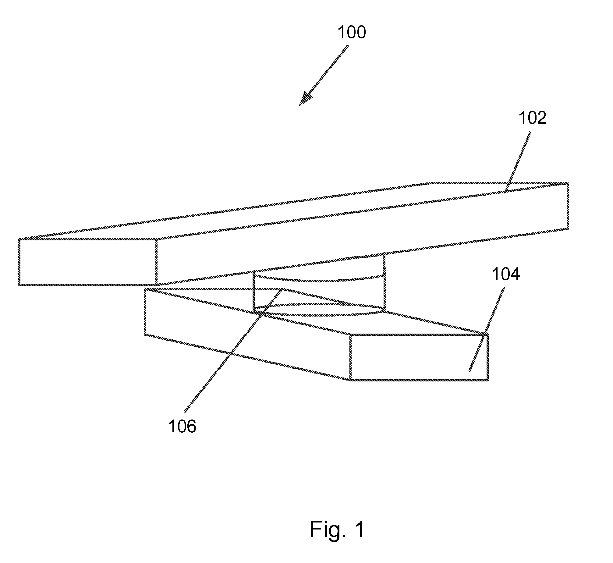
[0018]The present invention is in general related to two terminal devices. More particularly, embodiments of the present provide a method and a structure for a two terminal switching device. The two terminal switching device may be used in non-volatile resistive switching memory devices that provide for random access, fast switching, and are scalable to very small sizes. But it should be recognized that the present invention can have a much broader range of applicability.

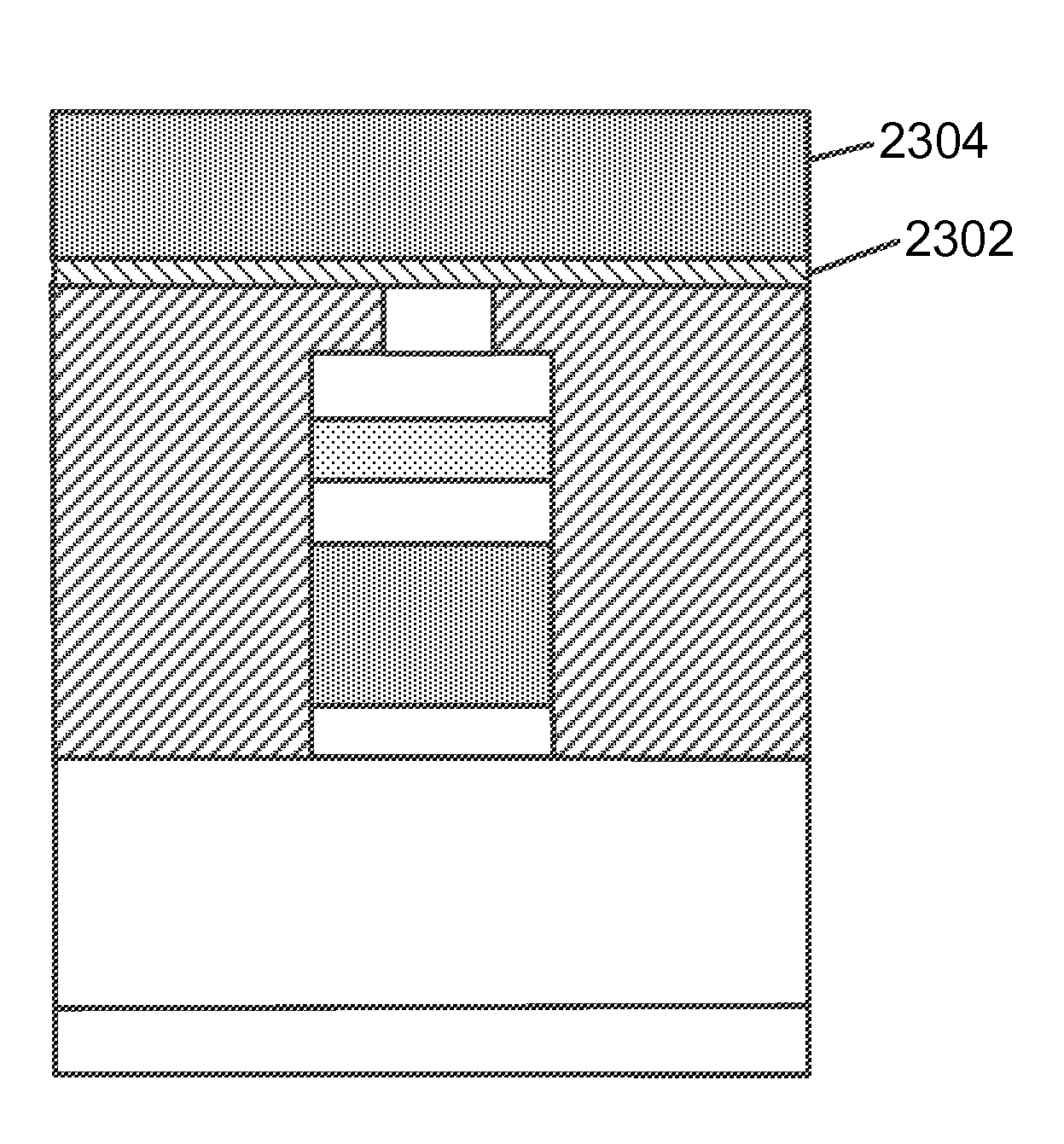
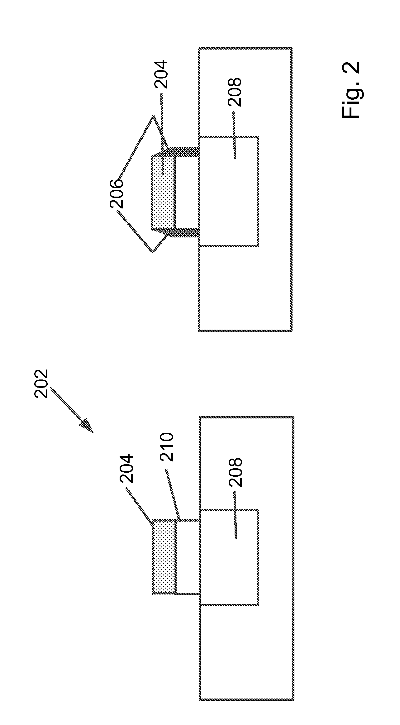
[0019]For switching devices using resistive switching, selected materials are used for each of the electrodes or the wiring structures. For example, a noble metal such as platinum is used for a nickel oxide-based resistive switching device to provide an ohmic contact to the device and to prevent chemical reaction with the switching material. Certain solid electrolyte based (for example, GeSe) switching devices or amorphous silicon based switching devices use silver as at least one of the electrode materials or conta...


PUM


Abstract

A method of forming a two terminal device. The method includes forming a first dielectric material overlying a surface region of a substrate. A bottom wiring material is formed overlying the first dielectric material and a switching material is deposited overlying the bottom wiring material. The bottom wiring material and the switching material is subjected to a first patterning and etching process to form a first structure having a top surface region and a side region. The first structure includes at least a bottom wiring structure and a switching element having a first side region, and a top surface region including an exposed region of the switching element. A second dielectric material is formed overlying at least the first structure including the exposed region of the switching element. The method forms an opening region in a portion of the second dielectric layer to expose a portion of the top surface region of the switching element. A top wiring material including a conductive material is formed overlying at lease the opening region such that the conductive material is in direct contact with the switching element. A second etching process is performed to form at least a top wiring structure. In a specific embodiment, the side region of the first structure including a first side region of the switching element is free from a contaminant conductive material from the second etching process.

Description

CROSS REFERENCE TO RELATED APPLICATIONS[0001]N / ASTATEMENT RELATED TO FEDERALLY SPONSORED RESEARCH OR DEVELOPMENT[0002]N / AREFERENCE TO A “SEQUENCE LISTING,” A TABLE, OR A COMPUTER LISTING APPENDIX SUBMITTED ON A COMPACT DISC[0003]N / ABACKGROUND[0004]The present invention is in general related to two terminal devices. More particularly, embodiments of the present provide a method and a structure for a two terminal switching device. The two terminal switching device can be used as a non-volatile resistive switching memory with random access and fast switching characteristics.[0005]The success of semiconductor devices has been mainly driven by an intensive transistor down-scaling process. However, as field effect transistors (FET) approach sizes less than 100 nm, problems such as short channel effect start to prevent proper device operation. Moreover, such sub 100 nm device size can lead to sub-threshold slope non-scaling and also increases power dissipation. It is generally believed tha...

Claims


Application Information

Patent Timeline
IPC IPC(8): H01L21/02
CPCH01L45/085H01L45/1233H01L45/16H01L45/1675H01L45/1253H01L45/148H10N70/245H10N70/841H10N70/826H10N70/884H10N70/011H10N70/063H10N70/20H10N70/8825H10N70/061H10B63/30H10N70/881H10N70/8416
Inventor JO, SUNG HYUNHERNER, SCOTT BRAD
Owner CROSSBAR INC
Why Eureka
Try Eureka