Non-lithographic formation of three-dimensional conductive elements

a technology of conductive elements and non-lithographic formation, which is applied in the direction of semiconductor devices, semiconductor/solid-state device details, electrical equipment, etc., can solve the problems of cumbersome development of masks for use in photolithography, inefficient and inaccurate photolithography,

Active Publication Date: 2012-01-26
TESSERA INC
View PDF9 Cites 144 Cited by
  • Summary
  • Abstract
  • Description
  • Claims
  • Application Information

AI Technical Summary

Problems solved by technology

Photolithography is inefficient and inaccurate when forming conductive traces simultaneously along multiple surfaces that are not parallel with one another.
It is cumbersome to develop a mask for use in photolithography that takes into account the surface changes of a substrate, or alternatively, to reposition and reorient the substrate to accommodate its differently-facing surfaces.

Method used


Image

  • Non-lithographic formation of three-dimensional conductive elements
  • Non-lithographic formation of three-dimensional conductive elements
  • Non-lithographic formation of three-dimensional conductive elements

Examples


first embodiment

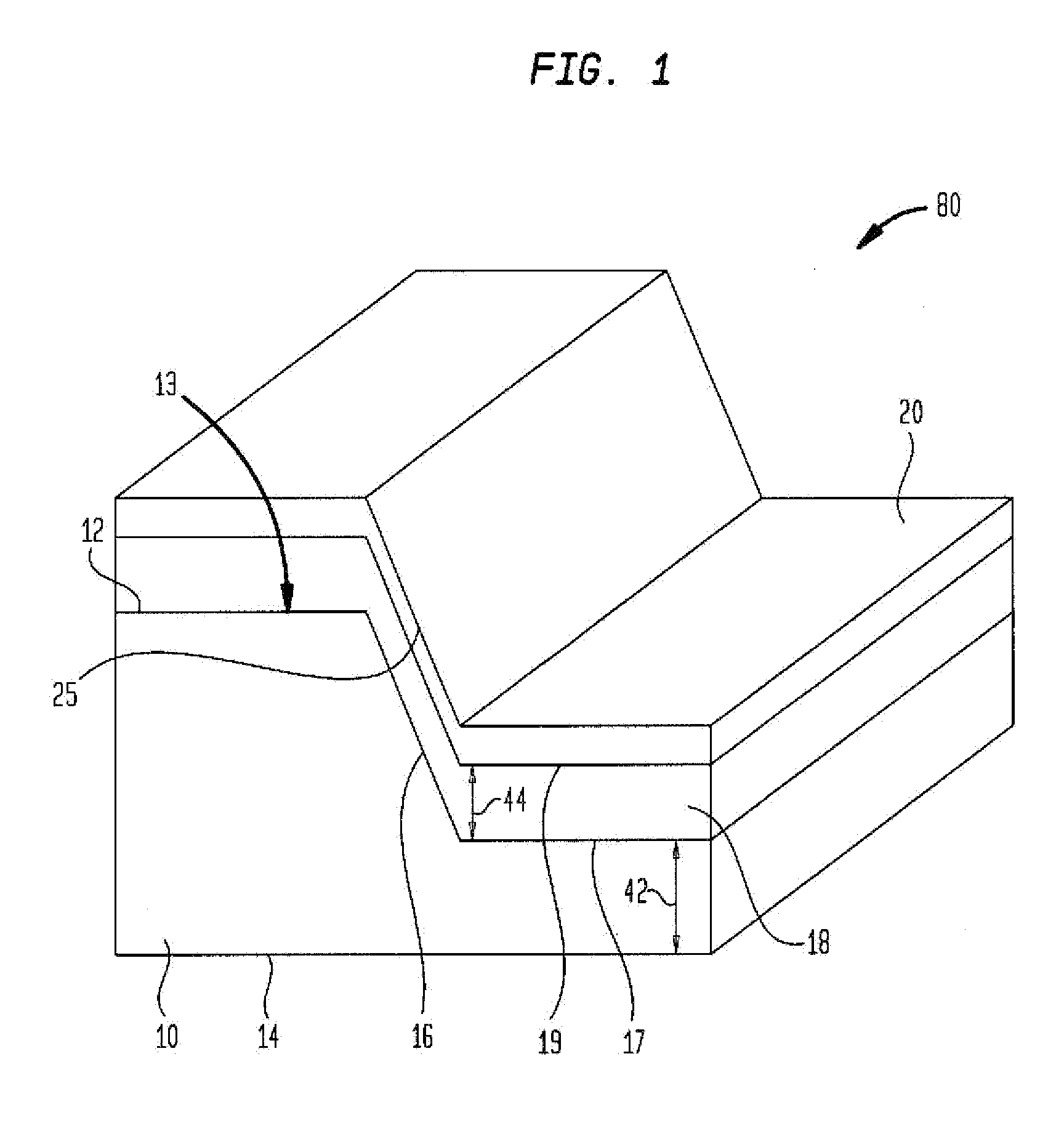
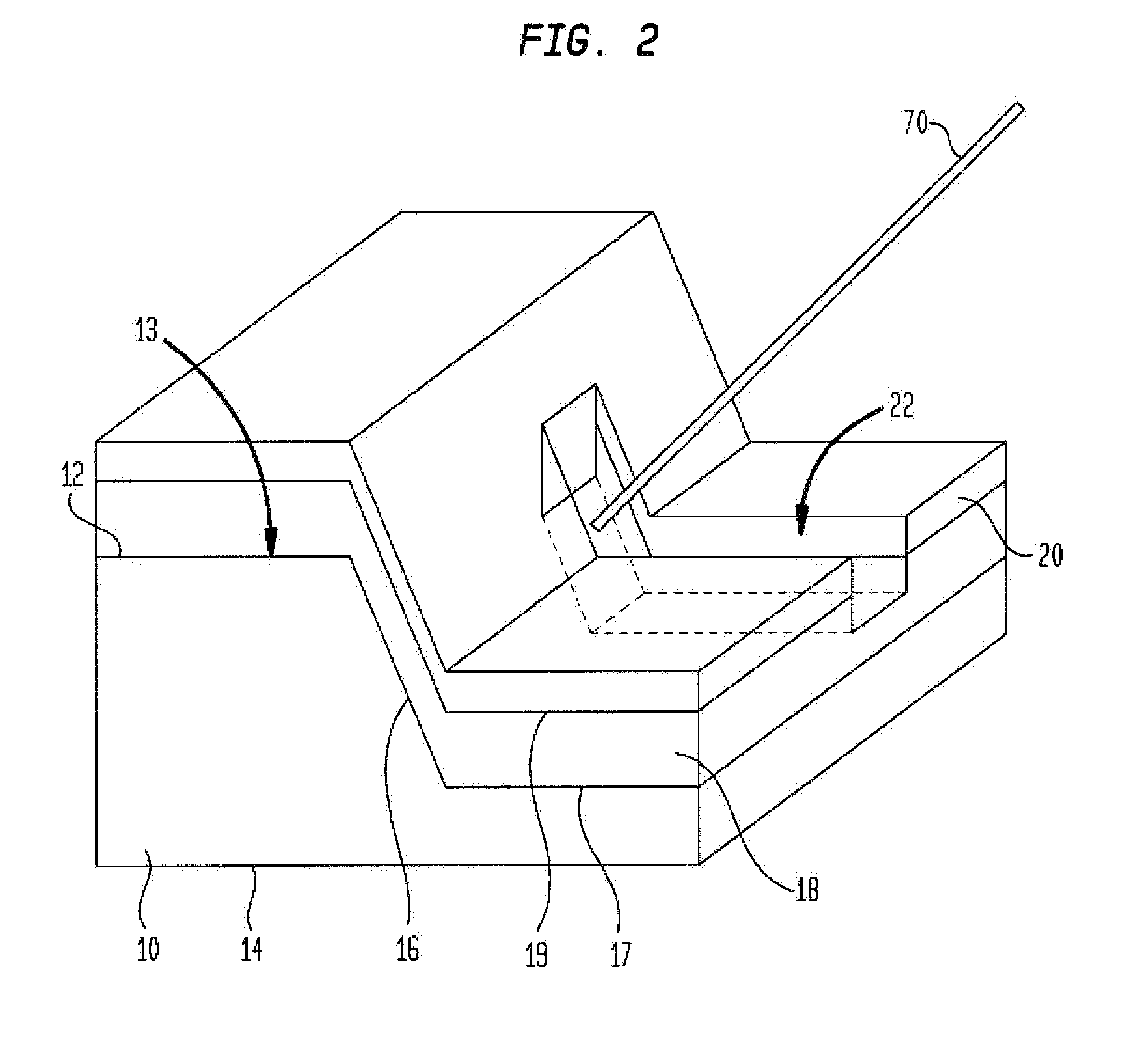
[0042]a semiconductor element 90, shown in FIG. 6, will be herein described according to its method of construction. An assembly 80 is shown in FIG. 1 having a substrate 10 with a rear face 12 and a front face 14. The substrate typically consists essentially of a monocrystalline semiconductor material such as, for example, silicon, an alloy of silicon with another material, one or more III-V semiconductor compounds such as gallium arsenide among others, or one or more II-VI semiconductor compounds. In a particular embodiment, the substrate can be a silicon-on-insulator substrate which includes a buried oxide (“BOX”) layer that separates an active semiconductor device layer at front face 14 from a bulk semiconductor region at rear face 12. A sloped surface 16 extends from rear face 12 toward front face 14, and a trench surface 17 extends from sloped surface 16. Rear face 12, sloped surface 16, and trench surface 17 will be referred to herein collectively as lower face 13. As describe...

second embodiment

[0050]an assembly is shown in FIGS. 7 and 8. Assembly 190 includes similar components to those described above, namely a substrate 110 with a rear face 112 and a front face 114. The substrate 110 can be a semiconductor element, such as can include microelectronic devices therein, such as in a microelectronic device region 160 adjacent the front face 114. Trenches 128 are formed in substrate 110 and are each defined by a trench surface 117 and sloped surfaces 116 extending from rear face 112 toward front face 114. Trenches 128 extend through much of the thickness of substrate 110 measured between rear face 112 and front face 114, and vias 121 extend from within the trenches 128 to contacts 155 at rear face 112. As seen in FIGS. 7-8, the trenches 128 are disposed adjacent peripheral edges 176 of the substrate 110 and can extend in directions parallel thereto.

[0051]Trenches 128 can alternatively be provided in the form of holes overlying individual ones of the vias 121, or in the form ...

third embodiment

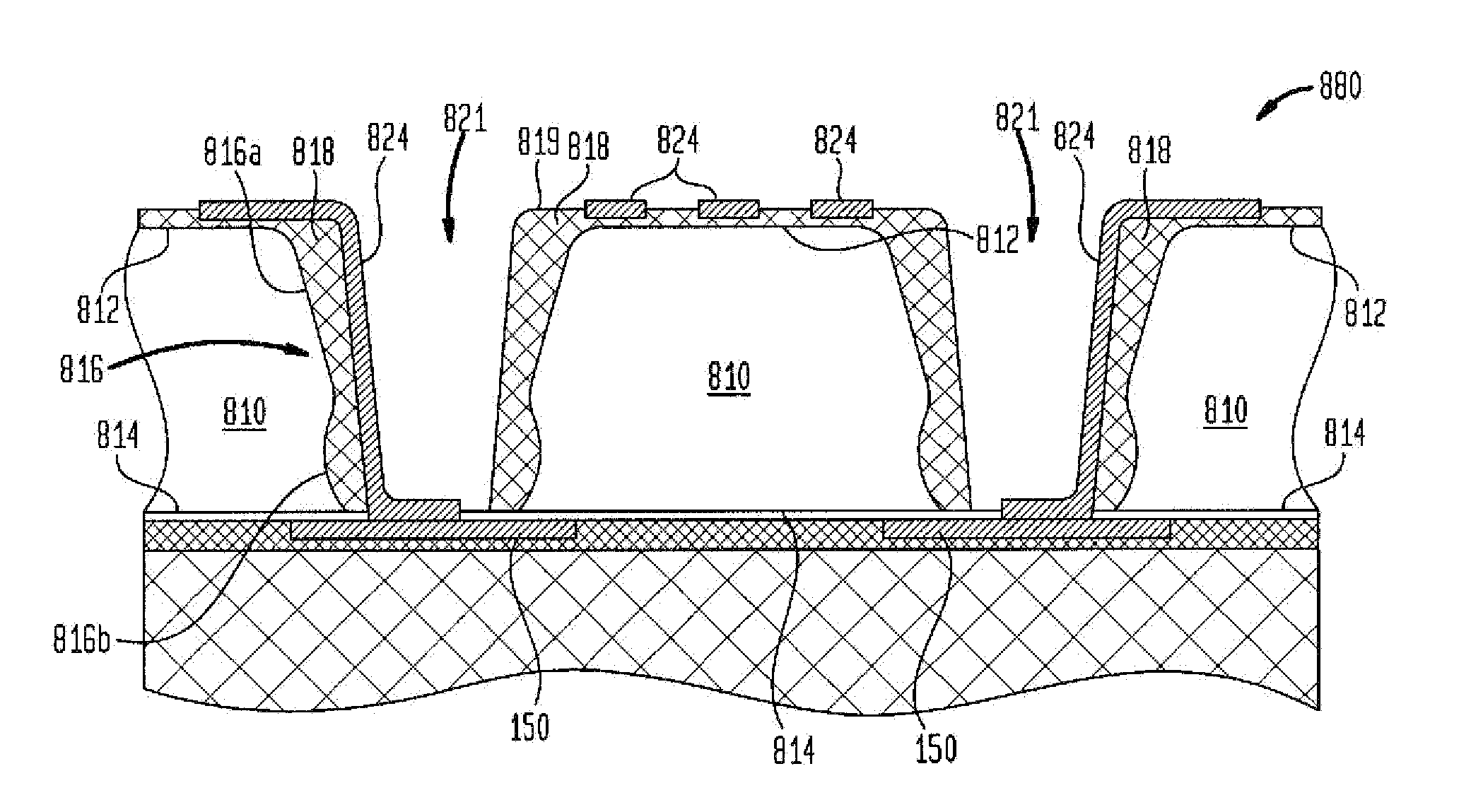
[0055]An assembly 290 is shown in FIGS. 10 and 11. Assembly 290 can include similar components to those described above, namely a substrate 210 with a rear face 212 and a front face 214. Substrate 210 further includes sloped surfaces 216 that extend from rear face 212 toward front face 214. A dielectric region 218 is provided overlying at least sloped surface 216. A conductive region overlies at least the rear face 112 and sloped surfaces 216. Vias 221 can extend from within the trenches 228 to contacts 255 at rear face 212, which in the example of FIGS. 10 and 11 are filled with conductive material. A conductive trace 224 can extend along sloped surface 216 and electrically connects a conductive pad 250 at front face 214 with a contact 255 at rear face 212. Conductive elements 224 can extend from individual ones of the vias 221 upwardly along sloped surface 216 that may be shared by several vias. Multiple conductive traces 224 may extend between pad 250 and contact 255 and may ext...


PUM


Abstract

A method of forming a conductive element on a substrate and the resulting assembly are provided. The method includes forming a groove in a sacrificial layer overlying a dielectric region disposed on a substrate. The groove preferably extends along a sloped surface of the substrate. The sacrificial layer is preferably removed by a non-photolithographic method, such as ablating with a laser, mechanical milling, or sandblasting. A conductive element is formed in the groove. The grooves may be formed. The grooves and conductive elements may be formed along any surface of the substrate, including within trenches and vias formed therein, and may connect to conductive pads on the front and / or rear surface of the substrate. The conductive elements are preferably formed by plating and may or may not conform to the surface of the substrate.

Description

BACKGROUND OF THE INVENTION[0001]The present invention relates to packaging of microelectronic devices, especially the packaging of semiconductor devices.[0002]Microelectronic devices generally comprise a thin slab of a semiconductor material, such as silicon or gallium arsenide, commonly called a die or a semiconductor chip. Semiconductor chips are commonly provided as individual, prepackaged units. In some unit designs, the semiconductor chip is mounted to a substrate or chip carrier, which is in turn mounted on a circuit panel, such as a printed circuit board.[0003]The active circuitry is fabricated in a first face of the semiconductor chip (e.g., a front surface). To facilitate electrical connection to the active circuitry, the chip is provided with bond pads on the same face. The bond pads are typically placed in a regular array either around the edges of the die or, for many memory devices, in the die center. The bond pads are generally made of a conductive metal, such as copp...

Claims


Application Information

Patent Timeline
Patent Type & Authority Applications(United States)
IPC IPC(8): H01L23/498H01L21/768
CPCH01L21/76898H01L23/481H01L23/4985H01L23/5226H01L2924/1461H01L24/06H01L2924/00H01L2924/12042H01L2924/14H01L21/76802H01L21/76879
Inventor OGANESIAN, VAGEHABA, BELGACEMMOHAMMED, ILYASMITCHELL, CRAIGSAVALIA, PIYUSH
Owner TESSERA INC
Why Eureka
Try Eureka