Novel high-temperature non-volatile memory design

a non-volatile memory and high-temperature technology, applied in the field of memory circuits and integrated circuit processes for fabricating memory circuits, can solve problems such as serious constraints of gidl, and achieve the effect of preventing excess junction leakage curren

Inactive Publication Date: 2012-01-26
APLUS FLASH TECH
View PDF0 Cites 8 Cited by
  • Summary
  • Abstract
  • Description
  • Claims
  • Application Information

AI Technical Summary

Benefits of technology

[0022]An object of this invention is to provide nonvolatile memory driver circuits for minimizing leakage current resulting from operating a nonvolatile memory at elevated temperatures.
[0023]Another object of this invention is to provide a method for fabricating a nonvolatile memory array for minimizing leakage current resulting from operating a nonvolatile memory at elevated temperatures.
[0024]To accomplish at least one of these objects, in some embodiments a method for fabricating a high temperature integrated circuit includes forming a drain / source diffusion of a first conductivity type separate from a substrate and an edge of a field isolation layer such that a concentration of impurity at the edge of the field isolation layer decreases a leakage occurring with high voltage and high temperature applied to the source / drain diffusion.

Problems solved by technology

GIDL constitutes a serious constraint, with regards to off-state current, in scaled down complimentary metal-oxide-semiconductor (CMOS) devices for DRAM and / or EEPROM applications and scaled CMOS digital VLSI circuits.

Method used


Image

  • Novel high-temperature non-volatile memory design
  • Novel high-temperature non-volatile memory design
  • Novel high-temperature non-volatile memory design

Examples


Embodiment Construction

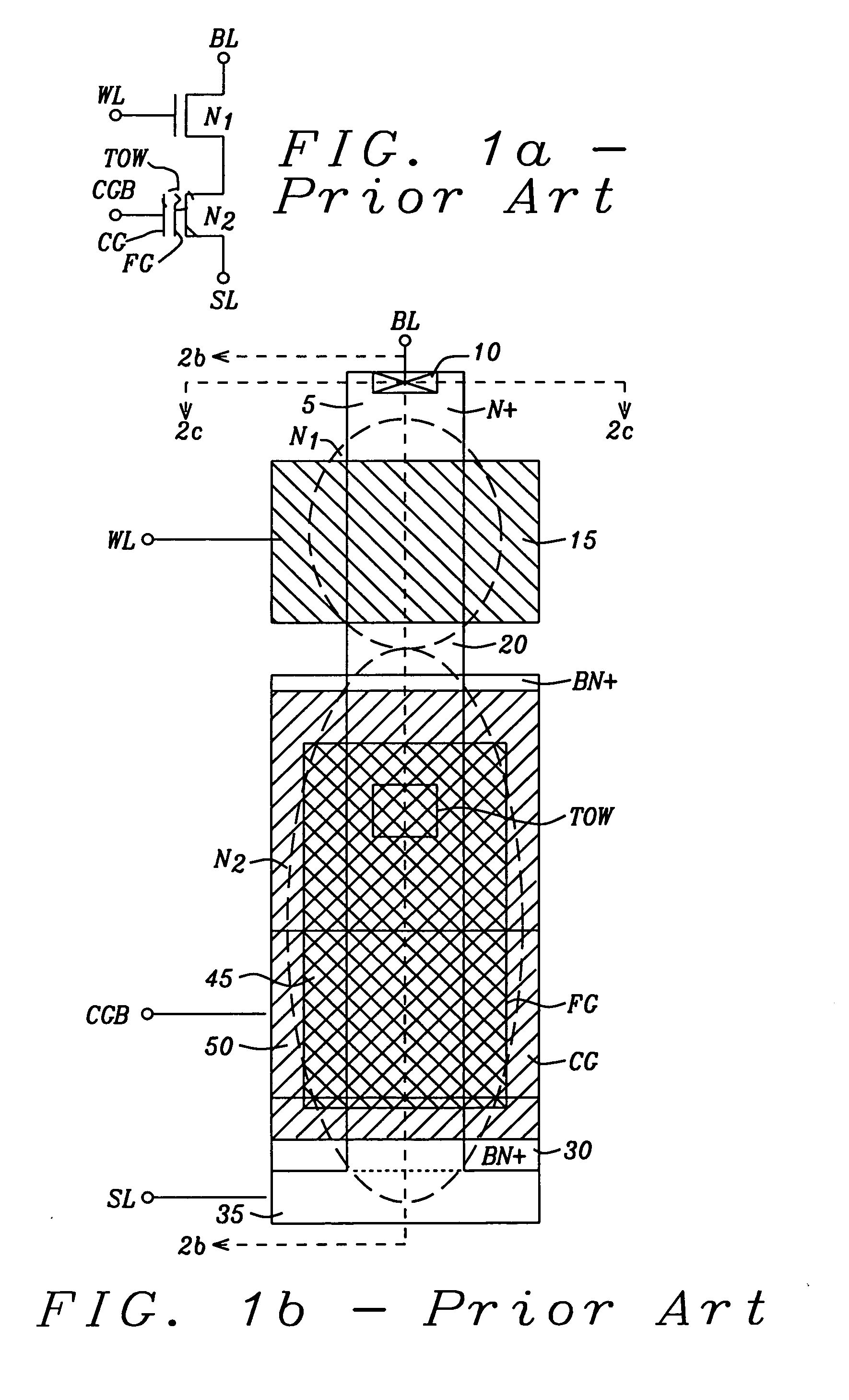
[0053]FIG. 1a illustrates the schematic circuit for a 2-transistor FLOTOX EEPROM cell of the prior art. The EEPROM cell of the prior art includes of two transistors N1 and N2. The select transistor, N1 is a polycrystalline silicon (polysilicon) NMOS device with its gate connected to a select gate signal SG. The source of the select transistor N1 is connected to the drain of the floating gate tunnel oxide (FLOTOX) EEPROM transistor N2. The FLOTOX EEPROM transistor N2 is a double polysilicon floating gate device. A first layer of polysilicon is the floating-gate FG that is used to store the charges representing the binary “0” and binary “1” of the stored data. The second layer of the polysilicon is a control gate CG that is connected to the word line WL. The drain of the select transistor N1 is connected to a vertical metal bit line BL. The source of the EEPROM transistor N2 is connected to a common horizontal implanted source line SL.

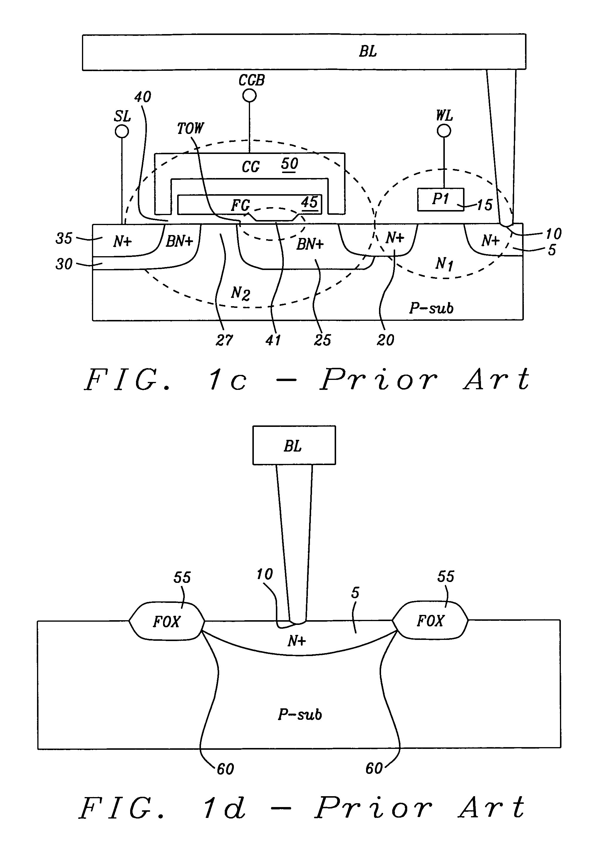
[0054]FIGS. 1b and 1c illustrate the physical layo...


PUM


Abstract

A method for fabricating a high temperature integrated circuit includes forming a drain / source diffusion and forming a buried diffusion implant containing the drain / source diffusion in a substrate to separate the drain / source diffusion from the substrate and an edge of a field isolation layer to decreases leakage current occurring with high voltage and high temperature. A nonvolatile memory array driver circuit with multiple driver transistors separated by anti-leakage transistors connected to prevent excess junction leakage current at elevated temperatures. Another nonvolatile memory array driver circuit has a high voltage blocking transistor connected to two anti-leakage transistors connected such that a source of the first anti-leakage transistor is connected to a drain of the high voltage blocking transistor and a drain of the second anti-leakage transistor is connected to prevent excess junction leakage current at elevated temperatures.

Description

[0001]This application claims priority under 35 U.S.C. §119 to U.S. Provisional Patent Application U.S. Provisional Patent Application Ser. No. 61 / 400,113, filed on Jul. 21, 2010, assigned to the same assignee as the present invention, and incorporated herein by reference in its entirety.BACKGROUND OF THE INVENTION[0002]1. Field of the Invention[0003]This invention relates generally to memory circuits and integrated circuit processes for fabricating memory circuits. More particularly, this invention relates to nonvolatile memory circuits and integrated processes for fabricating nonvolatile memory circuits capable of operation at high temperatures with low leakage currents.[0004]2. Description of Related Art[0005]In applications for automotive and military environments, integrated electronic circuits must be capable of operating in a high-temperature environment. The integrated electronic circuits must operate with no failure or decrease in operational specifications at an upper temp...

Claims


Application Information

Patent Timeline
Patent Type & Authority Applications(United States)
IPC IPC(8): G11C16/04H01L29/78H01L21/336
CPCG11C16/0433G11C16/08H01L27/0222H01L29/78H01L27/11536H01L27/11546H01L27/11519H10B41/10H10B41/44H10B41/49
Inventor LEE, PETER WUNGHSU, FU-CHANG
Owner APLUS FLASH TECH
Why Eureka
Try Eureka