

Driving circuit of insulated gate device
a technology of driving circuit and insulated gate, which is applied in the direction of oscillator generator, electronic switching, pulse technique, etc., can solve the problems of increasing the consumption power of the power mosfet, reducing the conductivity ability, and not taking measures against the case of sudden increase in power supply voltage, so as to prevent faulty turning on and reduce the chip size , the effect of high speed turning o
- Summary
- Abstract
- Description
- Claims
- Application Information
AI Technical Summary
Benefits of technology
Problems solved by technology
Method used
Image

Examples
Embodiment Construction
[0046]In the following, an embodiment of the invention will be explained on the basis of the attached drawings.
(Configuration)
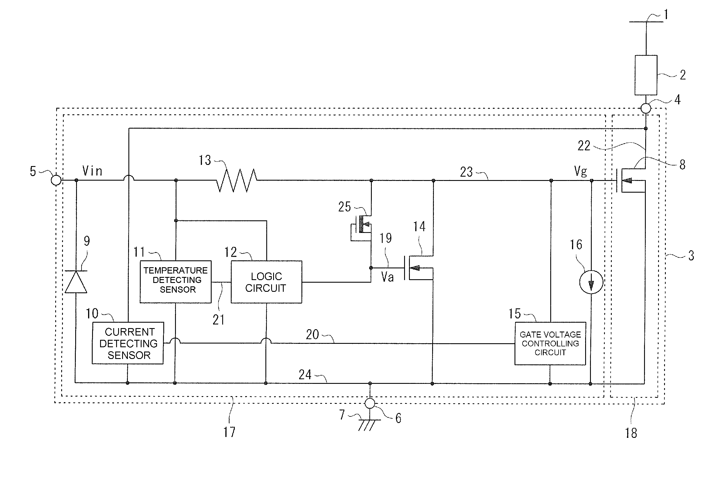
[0047]FIG. 1 is a circuit diagram showing the circuit configuration of a semiconductor integrated circuit system to which a driving circuit of an insulated gate device according to the invention is applied.
[0048]As is shown in FIG. 1, one end of a load 2, such as a resistive load or an inductive load, is connected to a power supply 1 and the other end of the load 2 is connected to a load driving control device 3 as a semiconductor integrated circuit system.
[0049]The load driving control device 3 is provided with three terminals of a drain terminal 4, a gate terminal 5 and a source terminal 6. The drain terminal 4 is connected to the other end of the load 2 and the source terminal 6 is connected to the ground 7. In addition, to the gate terminal 5, a gate signal is externally inputted. The load driving control device 3 is formed of a driving circuit unit 17 an...
PUM
 Abstract
Description
Claims
Application Information