Sampling and holding circuit, method of driving the same and imaging apparatus

a technology of sampling and holding circuit, which is applied in the direction of optical radiation measurement, pulse technique, instruments, etc., can solve the problems of increasing noise at the output terminal of the buffer, and achieve the effects of reducing noise, increasing sampling speed, and broader bandwidth

Inactive Publication Date: 2012-02-23
CANON KK
View PDF9 Cites 19 Cited by
  • Summary
  • Abstract
  • Description
  • Claims
  • Application Information

AI Technical Summary

Benefits of technology

[0005]However, a gain of a buffer depends on its bias current, and thus, the bandwidth becomes broader as its bias current becomes larger. Accordingly, an increase of the bias current of the buffer to provide a broader bandwidth in an attempt to increase the speed of the sampling and holding circuit operation results in an increase of noise at an output terminal of the buffer.

Problems solved by technology

Accordingly, an increase of the bias current of the buffer to provide a broader bandwidth in an attempt to increase the speed of the sampling and holding circuit operation results in an increase of noise at an output terminal of the buffer.

Method used


Image

  • Sampling and holding circuit, method of driving the same and imaging apparatus
  • Sampling and holding circuit, method of driving the same and imaging apparatus
  • Sampling and holding circuit, method of driving the same and imaging apparatus

Examples


first embodiment

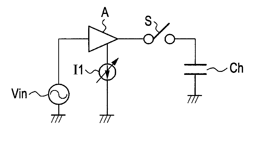
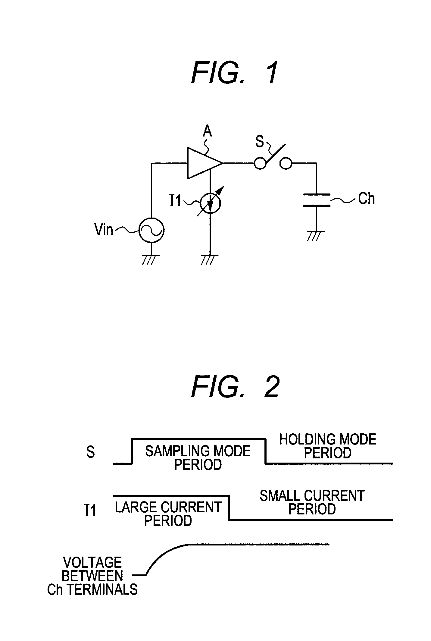
[0026]FIG. 1 is a diagram illustrating an example configuration of a sampling and holding circuit according to a first embodiment, and FIG. 2 is a timing diagram for the sampling and holding circuit. The Figures illustrate a buffer amplifier A that drives an input of a sampling and holding circuit including a switch S and a holding capacitor Ch, a bias current source I1 of a bias current for the buffer amplifier A, and a signal source Vin of a signal applied to an input of the buffer amplifier A. The buffer amplifier A amplifies the signal from the signal source Vin. The holding capacitor Ch stores the signal. The switch S is connected between an output terminal of the buffer amplifier A and the holding capacitor Ch.

[0027]FIG. 5 is a diagram illustrating an example configuration of the buffer amplifier A and the current source I1. The buffer amplifier A is a negative feedback circuit including a differential amplifier circuit 541, a common source amplifier circuit 543, and a phase c...

second embodiment

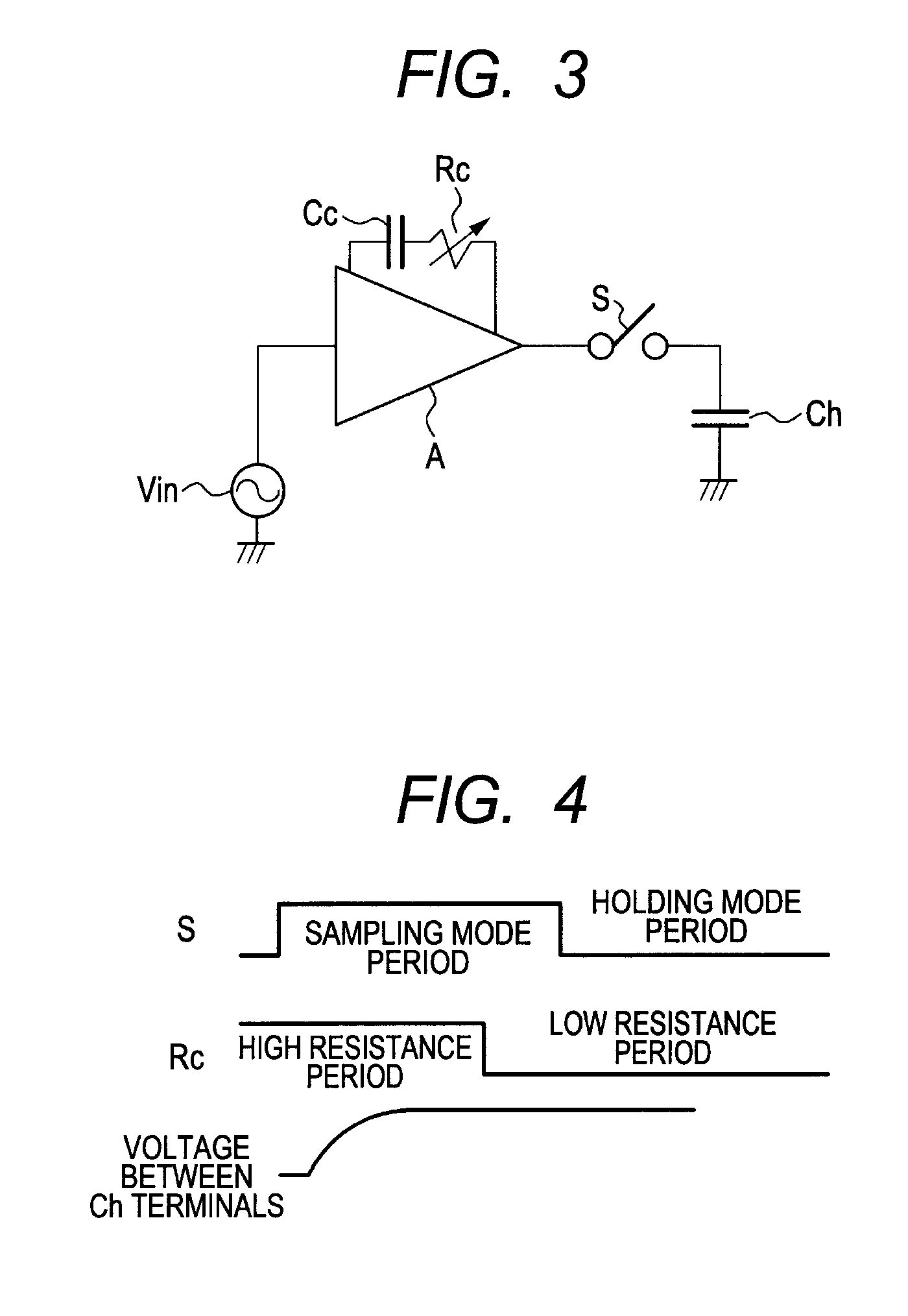
[0040]FIG. 3 is a diagram illustrating an example configuration of a sampling and holding circuit according to a second embodiment. Although the present embodiment is similar to the embodiment in FIG. 1, the present embodiment is different from the embodiment in FIG. 1 in that a variable resistor Rc whose resistance is variable according to timings of a sampling mode or a holding mode is connected in series to a phase compensation capacitor (or a capacitor for band limitation) Cc included in a buffer amplifier A and the current source I1 is deleted. A buffer amplifier A is a negative feedback circuit including a phase compensating circuit 542 (FIG. 5) including a circuit of serial connection of a capacitor Cc and a variable resistor Rc. During a certain period in which the sampling and holding circuit is in the sampling mode where a switch S is on as illustrated in the timing diagram in FIG. 4, the resistor Rc is set to have a high value to make the buffer amplifier A enter a board ...

third embodiment

[0043]FIG. 7 is a diagram illustrating an example configuration of a buffer amplifier A according to a third embodiment. The buffer amplifier A according to the present embodiment is provided in place of the buffer amplifier A and the current source I1 in FIG. 1. This is a case where the buffer amplifier A is an NMOS source follower amplifier, not an operational amplifier to which negative feedback is applied. First, a brief description will be given with reference to FIG. 7. The Figure illustrates an MOS transistor M7, which provides a source follower amplifier, a bias current source 14 for the MOS transistor M7, an output load capacitor C2, an MOS transistor M8, a voltage source VA that drives a gate of the MOS transistor M8, and a capacitor C3.

[0044]Where an MOS source follower amplifier is used as a drive circuit that drives a sampling and holding circuit, a pole frequency ωp in a gain-frequency characteristic of the MOS source follower amplifier can be represented by expression...


PUM


Abstract

A sampling and holding circuit includes an amplifier (A) that amplifies a signal, a holding capacitor (Ch) that stores the signal, and a switch (S) connected between an output terminal of the amplifier and the holding capacitor. In a state in which the switch is on, the amplifier amplifies the signal with a first signal bandwidth, and subsequently, in a state in which the switch is on, the amplifier amplifies the signal with a second signal bandwidth, which is narrower than the first signal bandwidth, and subsequently the switch is turned off while the amplifier still amplifies the signal with the second signal bandwidth.

Description

BACKGROUND OF THE INVENTION[0001]1. Field of the Invention[0002]The present invention relates to a sampling and holding circuit, a method of driving the circuits and an imaging apparatus.[0003]2. Description of the Related Art[0004]Japanese Patent Application Laid-Open No. 2006-345280 discloses a double sampling circuit used in an image sensor. In most recent analog signal processing circuits, a sampling and holding circuit using a switch and a capacitor is used. There is a demand for high speed operation not only in imaging sensors, but also in almost all electronic apparatuses, requiring a sampling and holding circuit in a signal processing circuit to operate at high speed. In order for a sampling and holding circuit to operate at high speed, it is necessary to broaden a signal bandwidth of a buffer that drives an input terminal of the sampling and holding circuit. Ordinarily, a signal bandwidth of a buffer, which depends on the bias current thereof, becomes broader as its bias cu...

Claims


Application Information

Patent Timeline
Patent Type & Authority Applications(United States)
IPC IPC(8): G11C27/02G01J1/44
CPCG11C27/026G01J1/46
Inventor SAKURAGI, TAKAMASA
Owner CANON KK
Why Eureka
Try Eureka