Method for treating group III nitride semiconductor
- Summary
- Abstract
- Description
- Claims
- Application Information
AI Technical Summary
Benefits of technology
Problems solved by technology
Method used
Image

Examples
first embodiment
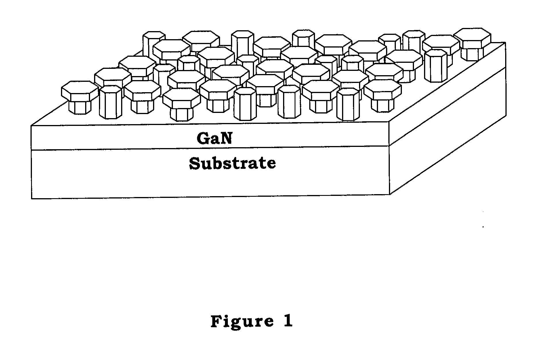
[0040]Heat the GaN template grown by Metal-organic Chemical Vapor Deposition (MOCVD) in the Hydride Vapor Phase Epitaxy (HVPE) reactor. When the temperature reaches about 1100° C. to 1000° C. (1050° C. is preferred and maintained at 1050° C.), introduce 3.95 standard liters per minute (slm) of nitrogen and 1.95 slm of hydrogen into the HVPE reactor. The pressure is maintained at about 750 torr to 650 torr (700 torr is preferred). The reaction time is about 5 minutes to 15 minutes (10 minutes is preferred). When the time is up, stop to supply hydrogen gas and reduce the temperature, the pattern shown in FIG. 1 will be formed on GaN surface.
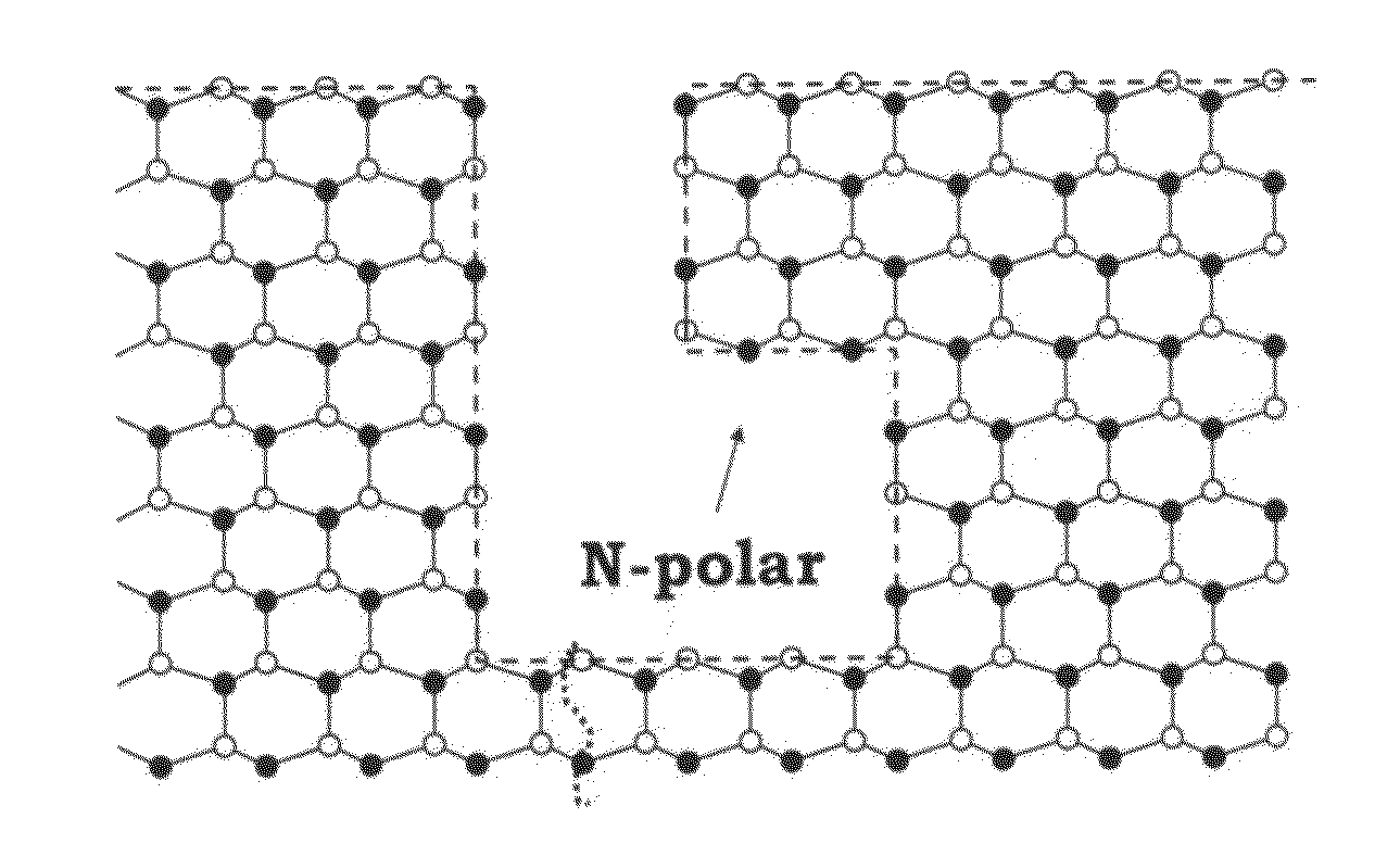
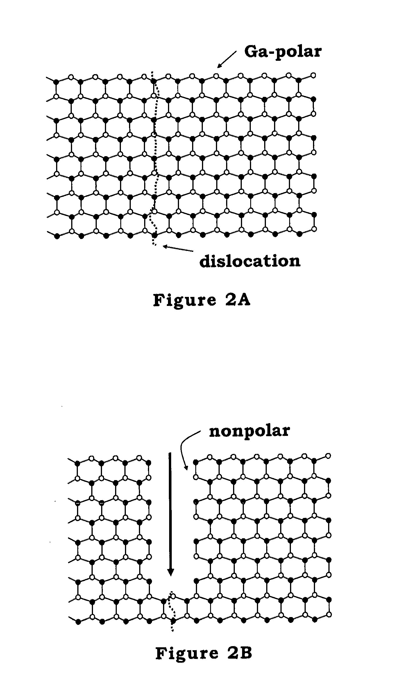
[0041]FIG. 1 shows the pattern etched by the invention. The surface pattern of GaN is caused by the etching of hydrogen. The nitrogen is only used as the environmental gas in the invention. Other inert gases are able to be used, such as argon, helium etc. Even when some equipments are used, only the etching gas is required without using other envir...
second embodiment
[0050]Heat the GaN template grown by Metal-organic Chemical Vapor Deposition (MOCVD) in the Hydride Vapor Phase Epitaxy (HVPE) reactor. When the temperature reaches about 1150° C. to 1050° C. (1100° C. is preferred and maintained at 1100° C.), introduce 3.95 standard liters per minute (slm) of hydrogen into the HVPE reactor. The pressure is maintained at about 750 torr to 650 torr (700 torr is preferred). The reaction time is about 5 minutes to 15 minutes (10 minutes is preferred). When the time is up, stop to supply hydrogen gas and reduce the temperature, the pattern shown in FIG. 1 will be formed on GaN surface. However, the etching depth and column size will be different from the results of the first embodiment.
[0051]As shown in FIG. 6, FIG. 7, and FIG. 8, the top view, the oblique view, and the side view for the patterns of the second embodiment are illustrated by the scanning electron microscope (SEM), respectively.
third embodiment
[0052]Heat the free-standing GaN substrate in the Hydride Vapor Phase Epitaxy (HVPE) reactor. When the temperature reaches about 1150° C. to 1050° C. (1100° C. is preferred and maintained at 1100° C.), introduce 5.9 standard liters per minute (slm) of hydrogen into the HVPE reactor. The pressure is maintained at about 750 torr to 650 torr (700 torr is preferred). The reaction time is about 25 minutes to 35 minutes (30 minutes is preferred). When the time is up, stop to supply hydrogen gas and reduce the temperature, the pattern shown in FIG. 1 will be formed on GaN surface. However, the etching depth and column size will be different from the results of the first embodiment and second embodiment. FIG. 9 shows the side view for the patterns of the third embodiment by the scanning electron microscope (SEM).
PUM
 Abstract
Description
Claims
Application Information
 - Generate Ideas
- Intellectual Property
- Life Sciences
- Materials
- Tech Scout
- Unparalleled Data Quality
- Higher Quality Content
- 60% Fewer Hallucinations
Browse by: Latest US Patents, China's latest patents, Technical Efficacy Thesaurus, Application Domain, Technology Topic, Popular Technical Reports.
© 2025 PatSnap. All rights reserved.Legal|Privacy policy|Modern Slavery Act Transparency Statement|Sitemap|About US| Contact US: help@patsnap.com