Manufacturing method of display device

a display device and manufacturing method technology, applied in the field of manufacturing methods of display devices, can solve the problems of reducing the productivity of coating films, affecting and material sensitivity is extremely low, so as to reduce the light transmittance of organic passivation films, reduce the time for forming organic passivation films, and improve the efficiency of liquid crystal display devices.

Active Publication Date: 2012-04-05
HITACHI DISPLAYS +1
View PDF3 Cites 11 Cited by
  • Summary
  • Abstract
  • Description
  • Claims
  • Application Information

AI Technical Summary

Benefits of technology

[0036]According to the invention, since the step time for forming the organic passivation film can be shortened, the productivity of the liquid crystal display device can be improved. Further, according to the invention, since the lowering of the light transmittance of the organic passivation film can be supp

Problems solved by technology

Organic insulating film resists conventionally used (organic passivation film materials) is prepared by adding photosensitive naphtoquinone diazide (hereinafter referred to as NQD) to acrylic resins but such materials have extremely low sensitivity and involve a problem with productivity.
Since existent organic passivation film materials require an exposure dose three to six that of usual photoresists, the productivity is lowered significa

Method used


Image

  • Manufacturing method of display device
  • Manufacturing method of display device
  • Manufacturing method of display device

Examples


example 1

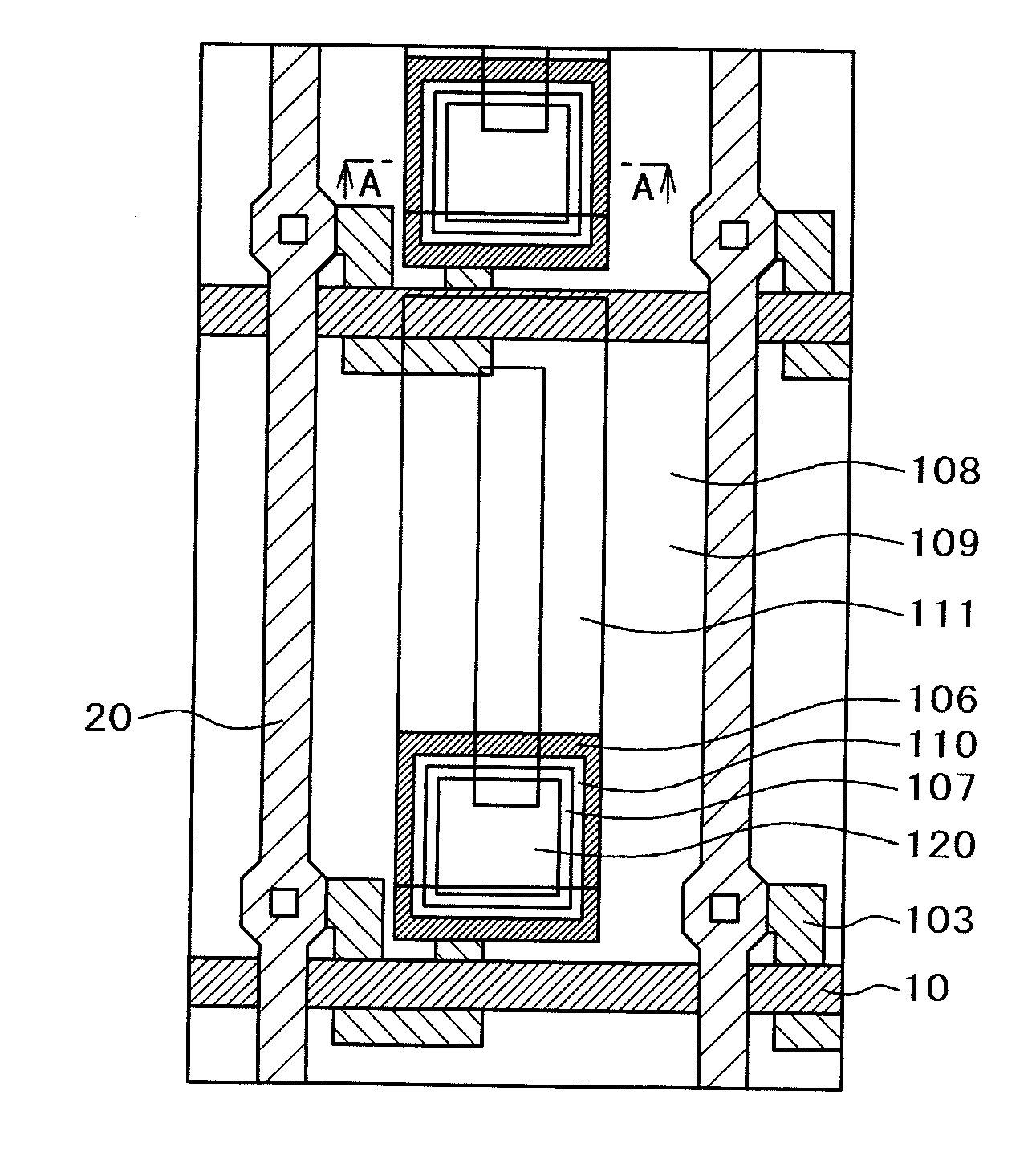
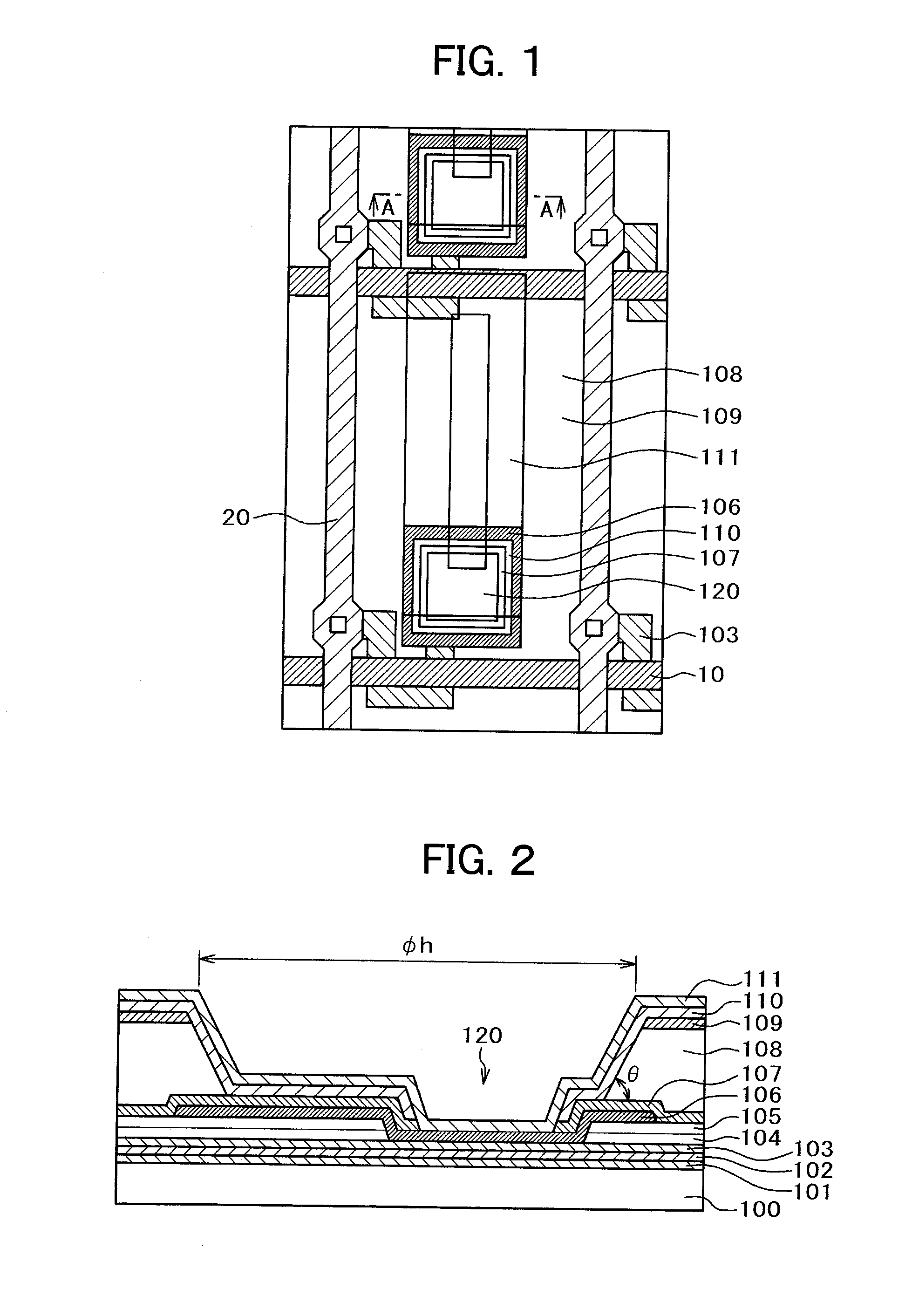
[0053]FIG. 1 is a plan view for a pixel portion of an IPS liquid crystal display device. In FIG. 1, signal lines 10 extend in the lateral direction, and video signal lines 20 extend in the longitudinal direction, being put an interlayer insulating film between them. A region surrounded by the scanning line 10 and the video signal 20 defines a pixel. A TFT, a pixel electrode 111, a counter electrode 109, etc. are formed in the pixel.

[0054]In FIG. 1, a semiconductor layer 103 is bent in a turned square U-shaped configuration and the scanning line 10 traverses the semiconductor layer 103 with a gate insulating film 104 being sandwiched between them. The scanning line 10 also serves as a gate electrode. A portion where the scanning line 10 and the semiconductor layer 103 intersect defines a channel of the TFT. One end of the semiconductor layer 103 is connected to the video signal line 20 and the video signal line 20 also serves as a drain electrode. The other end of the semiconductor l...


PUM


Abstract

An organic passivation film having a high transmittance and capable of setting a taper angle of a through hole within a predetermined range in a liquid crystal display device. A pixel electrode and a source electrode of a TFT are connected by way of a through hole formed in an organic passivation film. The organic passivation film having high productivity, high transmittance, and a predetermined taper angle θ of a through hole can be formed by using a chemical amplification photosensitive resin composition comprising, as a base material, an acrylic resin having a molecular weight of 4,000 to 20,000 and containing 1 to 6 wt % of a photoacid generator as the material for the organic passivation film, performing exposure and development for forming a through hole, and then performing post exposure, prebaking, and baking under appropriate conditions.

Description

CLAIM OF PRIORITY[0001]The present application claims priority from Japanese Patent Application JP 2010-225628 filed on Oct. 5, 2010, the content of which is hereby incorporated by reference into this application.BACKGROUND OF THE INVENTION[0002]1. Field of the Invention[0003]The present invention relates to a manufacturing method of a display device, particularly, a liquid crystal display device. The invention relates to a manufacturing method of a display device, particularly, a liquid crystal display device having high reliability and satisfactory productivity.[0004]2. Description of the Related Art[0005]A liquid crystal display device includes a TFT substrate having pixel electrodes, thin film transistors (TFT), etc. formed thereon in a matrix form, and a counter electrode opposing the TFT substrate and having color filters, etc. formed at positions corresponding to the pixel electrodes of the TFT substrate. Liquid crystals are put between the TFT substrate and the counter subst...

Claims


Application Information

Patent Timeline
IPC IPC(8): G03F7/20
CPCG03F7/40G03F7/0392
Inventor ISHIGAKI, TOSHIMASATAKAHASHI, FUMIOKANEKO, TOSHIKI
Owner HITACHI DISPLAYS
Why Eureka
Try Eureka