Magnetic memory element and driving method for same

a technology of magnetic memory and driving method, which is applied in the field of magnetic memory element, can solve the problems of large cell area, high accompanying bit cost, and devices that are not practical replacement technologies for dram, and achieve the effect of reducing the current density during switching

Active Publication Date: 2012-05-31
III HLDG 3
View PDF2 Cites 58 Cited by
  • Summary
  • Abstract
  • Description
  • Claims
  • Application Information

AI Technical Summary

Benefits of technology

[0022]By means of a magnetic memory element and driving method for such an element of this invention, the current density during

Problems solved by technology

Problems with this MRAM are a large cell area, and high accompanying bit cost.
If the cell area is from 20 to 30 F2 (where F is the minimum feature size of the manufacturing process) or larger, because of the excessive size, such devices are not practical as a replacement technology for DRAM.
However, in the structure first cited (Patent Reference 1), although lowering of the current density during switching can be expected, there is instead the problem that reliability as a nonvolatile memory element is worsened.
That is, during readout also the magnetic field leaking from the magnetic layer provided on the

Method used


Image

  • Magnetic memory element and driving method for same
  • Magnetic memory element and driving method for same
  • Magnetic memory element and driving method for same

Examples


Embodiment Construction

[0030]Below, embodiments of a magnetic memory element and driving method for such an element of the invention are explained based on the drawings.

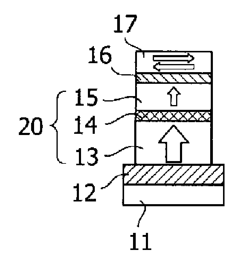
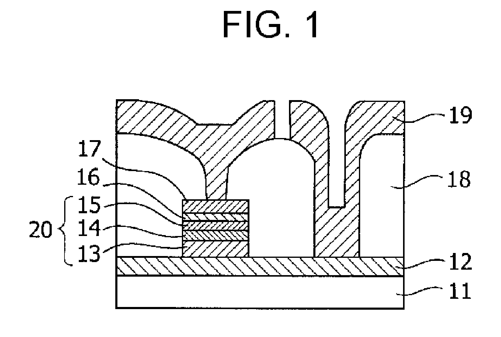
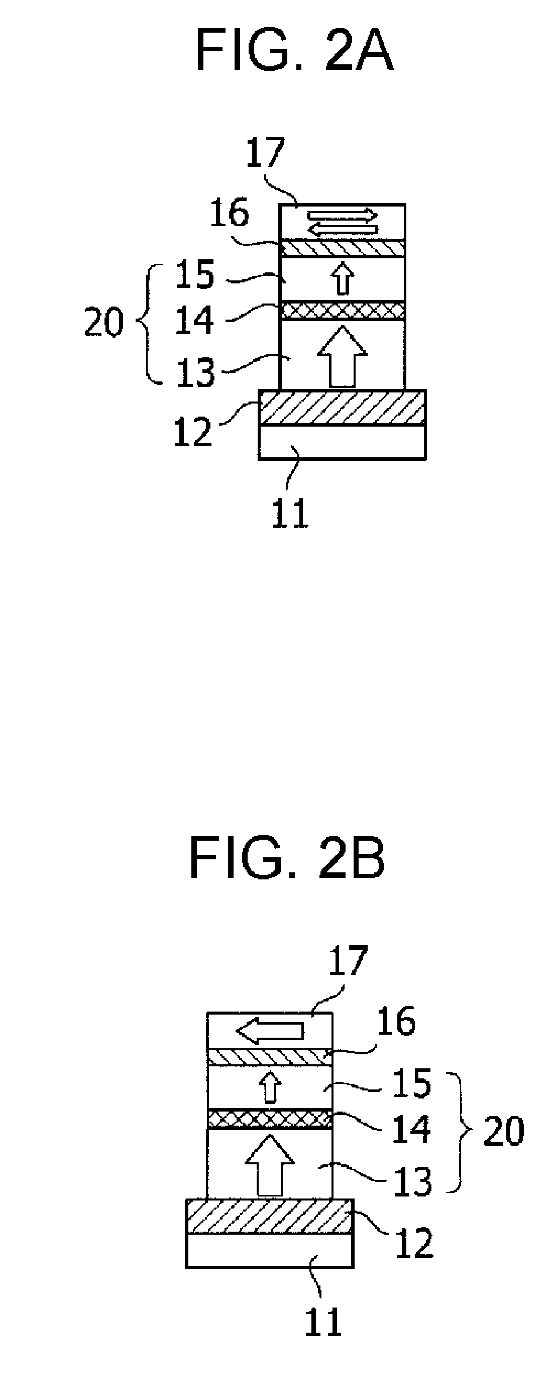
[0031]FIG. 1 is a cross-sectional view of a TMR (tunneling magnetoresistive) element used in a magnetic memory element of the invention. When manufacturing this TMR element, a sputtering method is used to form, in order on a substrate 11, a lower electrode 12, perpendicular magnetization pinned layer 13 comprising a perpendicular magnetization film, tunneling insulating film as a nonmagnetic layer 14, and perpendicular magnetization free layer 15 comprising a perpendicular magnetization film. Thereupon are formed a nonmagnetic metal layer 16 having a film thickness of 2 nm or less, and a phase transition in-plane magnetization film 17 having a film thickness of 20 nm.

[0032]In this embodiment, the lower electrode 12 is formed of Cu / Ta, the perpendicular magnetization pinned layer 13 is formed of FePt, the nonmagnetic layer 14 is formed of M...


PUM


Abstract

A magnetic memory element and a method of driving such an element are disclosed. The magnetic memory element has a magnetic tunnel junction portion with a spin-valve structure having a perpendicular magnetization free layer formed of a perpendicular magnetization film, a perpendicular magnetization pinned layer formed of a perpendicular magnetization film, and a nonmagnetic layer sandwiched between the perpendicular magnetization free layer and the perpendicular magnetization pinned layer, and records information by application of an electric pulse to the magnetic tunnel junction portion. An in-plane magnetization film, interposed in the path of the electric pulse, is disposed in the magnetic tunnel junction portion. The in-plane magnetization film is configured so as to exhibit antiferromagnetic (low-temperature)-ferromagnetic (high-temperature) phase transitions depending on temperature changes based on application of the electric pulse to the magnetic tunnel junction portion.

Description

TECHNICAL FIELD[0001]This invention relates to a magnetic memory element capable of storing information by electrical means, and a driving method for such an element.BACKGROUND ART[0002]In recent years there have been striking increases in the capacity of nonvolatile semiconductor storage devices, of which flash memory is representative, and products with capacities as great as 32 Gbytes have been announced. In particular, the product value of USB memory and storage for mobile phones is increasing. That is, nonvolatile semiconductor storage devices are inherently superior, in areas which are uniquely the realm of solid state element memory, such as resistance to vibration, high reliability, and low power consumption, and so are becoming the mainstream of storage devices for portable music and video content, and as storage for transportable electronic equipment.[0003]On the other hand, separately from the above storage, energetic research is being conducted to impart nonvolatile prop...

Claims


Application Information

Patent Timeline
IPC IPC(8): G11C11/16H01L29/82
CPCB82Y25/00H01F10/3254H01F10/3268H01F10/3286G01R33/093G01R33/098G11C11/161H01L43/08G11C11/1675G11C11/1673H10N50/10H10N50/01
Inventor OGIMOTO, YASUSHI
Owner III HLDG 3
Why Eureka
Try Eureka