Gate driver and semiconductor device employing the same

Active Publication Date: 2012-06-07
SANKEN ELECTRIC CO LTD
View PDF10 Cites 27 Cited by
  • Summary
  • Abstract
  • Description
  • Claims
  • Application Information

AI Technical Summary

Benefits of technology

[0007]The active clamp circuit mentioned in Patent Documents 1 and 2 generates and provides a clamp current through a gate resistance of the switching element when a gate drive signal is OFF, and thereby increasing a voltage drop of the gate resistance. When the voltage drop reaches a gate threshold voltage of the switching element, the switching e

Problems solved by technology

Then, the techniques mentioned in Patent Documents 1 and 2 are not adoptable because they must add a heat radiating means for the active clamp circuit, to increase costs and decrease reliability.
The

Method used


Image

  • Gate driver and semiconductor device employing the same
  • Gate driver and semiconductor device employing the same
  • Gate driver and semiconductor device employing the same

Examples


Example

[0018]Gate drivers and semiconductor devices according to embodiments and modifications of the present invention will be explained in detail with reference to the drawings.

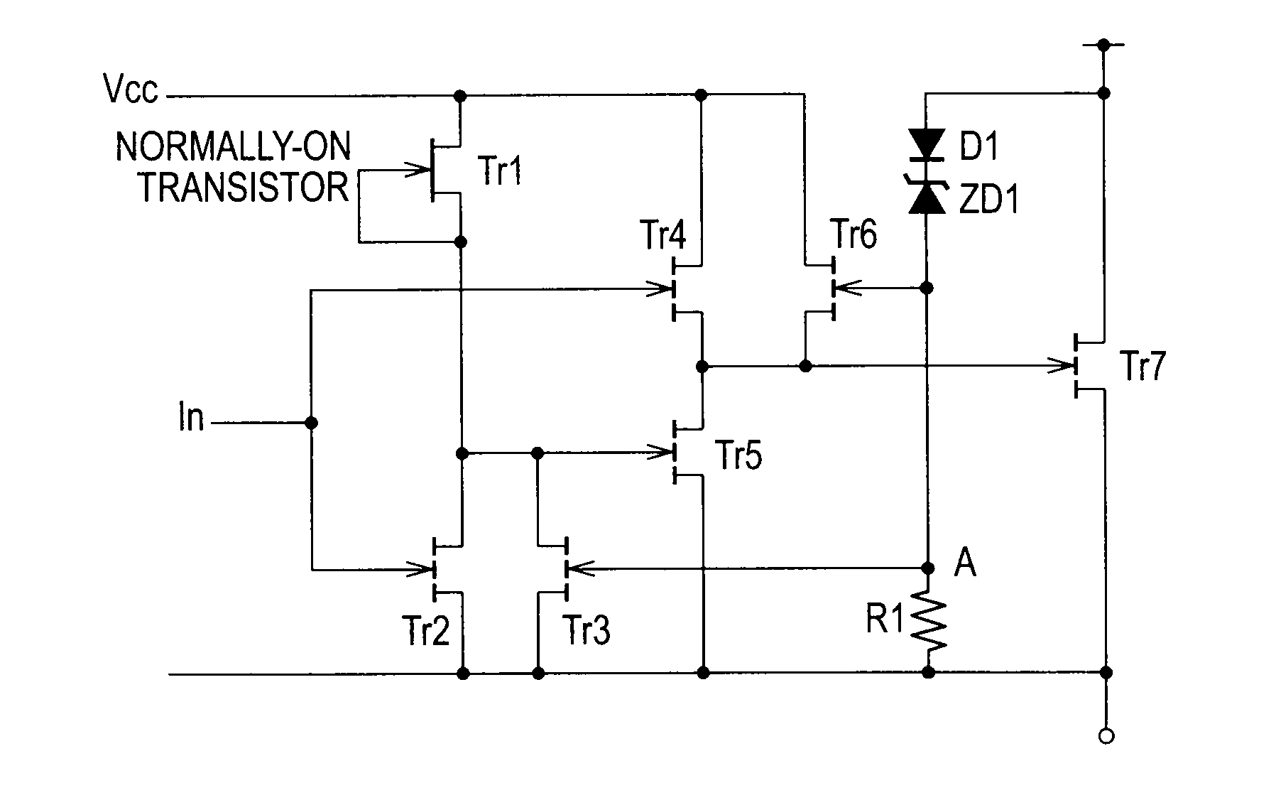
[0019]FIG. 1 is a circuit diagram illustrating a gate driver according to an embodiment of the present invention. The gate driver drives a switch element Tr7 and includes transistors Tr1 to Tr6, a diode D1, a zener diode ZD1, and a resistor R1. The switch element Tr7 corresponds to the “switching element” stipulated in the claims and is a semiconductor element such as a GaN HEMT. The gate driver and switch element Tr7 form a semiconductor device according to the preset embodiment.

[0020]According to the present embodiment, the transistors Tr1 to Tr6 may be n-type MOSFETs, or n-type GaN HEMTs, or any combination of other types of semiconductor elements that provide the function of the present embodiment.

[0021]The transistors Tr1, Tr2, Tr4, and Tr5 form the “driving part” stipulated in the claims, to drive the switch...


PUM


Abstract

A gate driver for driving a gate of a switching element Tr7 includes a driving part that drives the switching element according to a control signal and an active clamp circuit to clamp the voltage between the first and second main terminals of the switching element through the driving part. If a voltage applied between a first main terminal (drain) and a second main terminal (source) of the switching element exceeds a predetermined voltage, the active clamp circuit forcibly blocks a driving operation of the driving part from driving the switching element.

Description

BACKGROUND OF THE INVENTION[0001]1. Field of the Invention[0002]The present invention relates to a gate driver for driving the gate of a switching element and to a semiconductor device employing the gate driver.[0003]2. Description of Related Art[0004]Recent output transistors used in, for example, switching power sources carry out high-speed switching to cause a large counter electromotive voltage that produces a surge voltage between the drain and source of the output transistor when the transistor is turned off to open the drain and source thereof. Such a surge voltage may break the transistor, and therefore, the transistor must have a means to protect the transistor from the surge voltage.[0005]In connection with this, Japanese Unexamined Patent Application Publication No. H08-288817 (Patent Document 1) discloses a semiconductor device for disconnecting an inductive load at high speed from a high-side switch and a technique of suppressing a drain-source voltage of the high-side ...

Claims


Application Information

Patent Timeline
IPC IPC(8): G05F1/10
CPCH02M1/32H03K17/0822H02M3/33507H02M1/36
Inventor MACHIDA, OSAMUAOKI, HIRONORI
Owner SANKEN ELECTRIC CO LTD
Why Eureka
Try Eureka