
Bi-mode sense amplifier with dual utilization of the reference cells and dual precharge scheme for improving data retention

a data retention function and reference cell technology, applied in the field of bimode sense amplifiers with dual utilization of reference cells and dual precharge schemes for improving data retention, can solve the problems of excessive power consumption of data retention functions, degraded precharge schemes, and excessive power required to refresh memory cells, etc., to achieve power saving, reduce array device off current, and reduce drain-source voltage vds

Inactive Publication Date: 2006-05-16
IBM CORP
View PDF10 Cites 24 Cited by
  • Summary
  • Abstract
  • Description
  • Claims
  • Application Information

AI Technical Summary

Benefits of technology

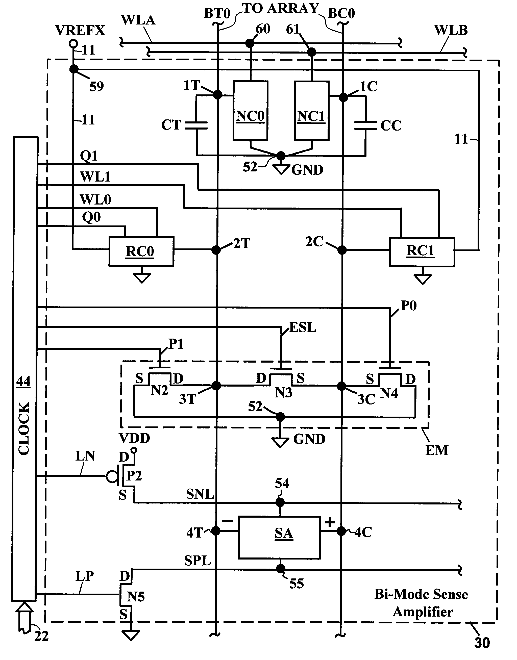
[0071]In addition to power savings, use of a VDD / X voltage such as VDD / 2 reduces drain-source voltage Vds of the array device in the precharge state; and subsequently a VDD / X voltage such as VDD / 2 reduces array device off current. That results in extended retention times and further decreases power consumption. To provide simultaneously a low power retention mode and a high performance active mode, it is desirable to enable the sense amplifier to operate in either a VDD / X precharge or GND precharge mode.

Problems solved by technology

Although a GND precharge sensing scheme can support a wider operating range and provides more overdrive during amplification and more precharge than conventional VDD / 2 sensing, it has the problem that it consumes more power.
However, a GND precharge scheme suffers from the problem of degraded retention characteristics for a stored ‘1’, where the drain to source voltage of the storage transistor is the worst case for leakage current through the storage transistor.
The first disadvantage is that data retention functions consume excessive power required to refresh the memory cell.
The second disadvantage is that memory availability is degraded because it is inaccessible during the time consumed by performance of the increased number of refresh cycles.
Therefore, both of the above GND and VDD sensing schemes, which present the problem of high cell leakage during the precharge condition, are not suitable for low power applications, even if such schemes show better performance and design robustness regardless of power supply voltage.
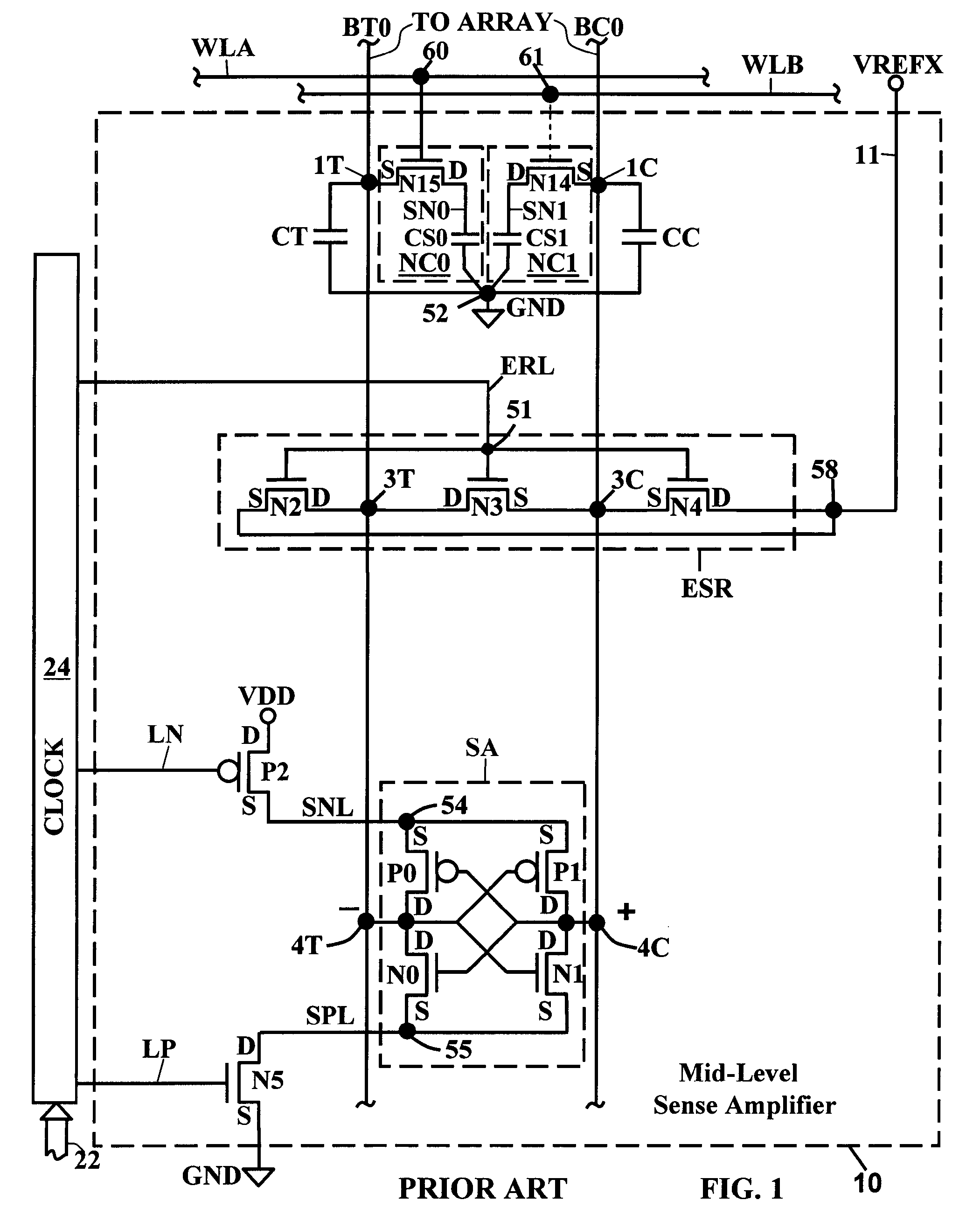
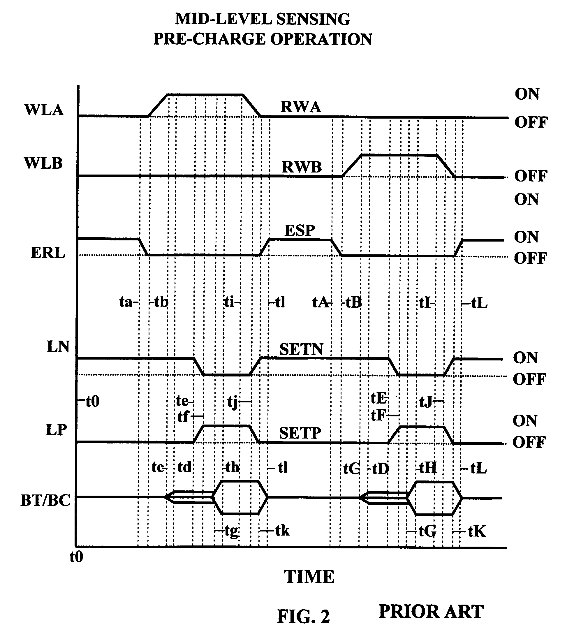
Although mid-level sensing offers better retention characteristics, performance thereof falls short of objectives.
That results in extended retention times and further decreases power consumption.

Method used


Image

  • Bi-mode sense amplifier with dual utilization of the reference cells and dual precharge scheme for improving data retention
  • Bi-mode sense amplifier with dual utilization of the reference cells and dual precharge scheme for improving data retention
  • Bi-mode sense amplifier with dual utilization of the reference cells and dual precharge scheme for improving data retention

Examples


first embodiment

[0087]FIG. 5 shows a combination of clock 44 and the bi-mode sense amplifier system 30 designed in accordance with this invention comprising a combination of features of the Mid-Level sense amplifier of FIG. 1 and the GND precharge system of FIG. 3 during the first phase of operation in which a true bitline normal cell NC0 and a complimentary bitline reference cell RC1 are activated to connect the storage capacitor CS0 to the true bitline BT0 in response to a true wordline pulse RWA on true wordline WLA. The true normal cell NC0 and the complementary normal cell NC1 are the same as in FIG. 1. The reference cell RC0 and the reference cell RC1 are the same as in FIG. 3. The reference cell RC0 and the reference cell RC0 and the reference cell RC1 are the same as in FIG. 3. The reference cell in this embodiment is used as the bitline precharge purpose.

[0088]FIG. 6A shows the signal timing diagrams of the GND precharge for the mission modes of operation of the circuit of FIG. 5. In addit...

second embodiment

[0098]FIG. 7 is the schematic diagram of a second embodiment of the present invention in which a combination of a clock 64 and a bi-mode sense amplifier system 40 includes dual precharge circuits, which is a modification of the bi-mode sense amplifier system as shown in FIG. 5. The true normal cell NC0 and the complementary normal cell NC1 are the same as in FIG. 1. Reference cell RC0 and reference cell RC1 are the same as in FIG. 3.

[0099]FIG. 7 is a schematic diagram of the combination of a clock 64 a dual precharge circuit 40 which includes a sense amplifier SA, plus thirteen other MOSFETs or two more FETs than for FIG. 5. The sense amplifier SA can be identical to the sense amplifier SA shown in FIG. 1 or can be modified to include another equivalent sense amplifier circuit.

[0100]FIG. 8 shows the signal timing diagram of wordline, equalization signal, equalization pulse, true bitline and complementary bitline potentials applied to and generated in the circuit of FIG. 7.

[0101]In F...

third embodiment

[0123]FIG. 9 is a schematic diagram of a third embodiment of the present invention in which a bi-mode sense amplifier system includes a MOSFET dual precharge circuit, which show a modification of the system as shown in FIG. 7. The true normal cell NC0 and the complementary normal cell NC1 are the same as in FIG. 1. The reference cell RC0, and the reference cell RC1 are all the same as in FIG. 3

[0124]FIG. 9 shows a modification of the circuit of FIG. 7 including a clock 84 and a system 50. System 50 includes fourteen transistors and four capacitors. The circuit inside the sense amplifier block SA can be identical to the sense amplifier SA shown in FIG. 1 or can be modified to include another equivalent sense amplifier circuit. Instead of the three equalization NFETs N2, N3 and N4 of the VREFX reference potential equalization circuit ESR in FIG. 7 that are tied to operate in response to the equalization signal on line EQS, in FIG. 8 there is a shorting equalization circuit ES which in...


PUM


Abstract

An electronic memory system includes a memory array of a number of pair of bitlines comprising a true bitline and a complementary bitline. A first normal cell connects to the true bitline (BT0) and a second normal cell connects to the complementary bitline (BC0). A first reference cell connects to the true bitline and a second reference cell connects to the complementary bitline. A clock generates timing pulses including short circuiting-equalization pulses and selectively provides reference potential pulses in a reference potential mode of operation. A sense amplifier has a true terminal connected to the true bitline and a complementary terminal connected to the complementary bitline. An equalization short circuiting circuit connects to the clock and to the true bitline and the complementary bitline for short circuiting the true bitline and the complementary bitline together in response to the short circuiting pulses to equalize the electric potential thereon as a function of short circuiting-equalization. A precharge circuit connects at least one of the true bitline and the complementary bitline to an electrical potential selected from a higher voltage or low voltage reference potential in response to a precharge equalization clock pulse from the clock generator.

Description

BACKGROUND[0001]In the operation of DRAM (Dynamic Random Access Memory) devices, it is required to maintain data stored in a charge storage cell for a maximum retention period without performing a refresh operation in order to offer high availability and low power consumption. When competing with Static RAM (SRAM) devices, it is also desirable to offer high performance with the same DRAM design. In the current state of the art there are DRAM designs that offer either high retention times for the stored data or high performance. The following art describes a scheme for offering both high retention times for the stored data and high performance with a single circuit configuration. Conventional mid-level sensing schemes precharge the bitlines to mid-level potentials such as VDD / 2, VDD / 3, or VDD / X (where VDD is power supply voltage and X is a number greater than 1) and offer good retention times for the stored data. Rail sensing schemes precharge the bitlines to VDD or ground (hereinaft...

Claims


Application Information

Patent Timeline
Patent Type & Authority Patents(United States)
IPC IPC(8): G11C7/00
CPCG11C7/065G11C7/12G11C11/4099G11C11/4091G11C11/4094G11C7/14
Inventor BARTH, JR., JOHN E.KIM, HOKI
Owner IBM CORP
Learn More