Method for manufacturing suspended fin and gate-all-around field effect transistor

a technology of field effect transistor and suspended fin, which is applied in the direction of transistors, semiconductor devices, electrical equipment, etc., can solve the problems of reducing the induced barrier, the leakage current between the source and the drain, and the problem of severe challenges for the planar cmos device on bulk silicon, etc., to achieve the elimination of the bottom leakage passage, the effect of easy integration and simple manufacturing process

Active Publication Date: 2012-06-14
INST OF MICROELECTRONICS CHINESE ACAD OF SCI
View PDF1 Cites 14 Cited by
  • Summary
  • Abstract
  • Description
  • Claims
  • Application Information

AI Technical Summary

Benefits of technology

[0022]2) The present invention relates to a method for manufacturing a suspended fin which can be implemented as a simple manufacture process, is easy to be integrated into and compatible with a planar CMOS process.
[0023]3) The present invention relates to a method for manufacturing a suspended fin which has an oxide layer as an isolation structure at the bottom, which can suppress a bottom parasitic transistor, eliminate a bottom leakage passage, and improve properties of the device.
[0024]4) The present invention relates to a method for manufacturing a gate-all-around device which can be implemented on a bulk silicon substrate, suppress a self-heating effect and a floating-body effect of the SOI substrate, and lower a manufacture cost.
[0025]5) The present invention relates to a method for manufacturing a gate-all-around device which can be implemented as a simple manufacture process, is easy to be integrated into and compatible with a planar CMOS process.
[0026]6) The present invention relates to a method for manufacturing a gate-all-around device which avoids selective epitaxial growth on source / drain regions or the like for reducing a series resistance in the source / drain regions, and reduces dependencies on manufacturing equipments, and can be easily implemented.

Problems solved by technology

A planar CMOS device on a bulk silicon is facing with severe challenges, such as a short channel effect (SCE), leakage current between the source and the drain, a drain induced barrier lowering effect (DIBL), and the like.
However, there are still many problems in manufacturing a gate-all-around device with an SOI substrate.

Method used


Image

  • Method for manufacturing suspended fin and gate-all-around field effect transistor
  • Method for manufacturing suspended fin and gate-all-around field effect transistor
  • Method for manufacturing suspended fin and gate-all-around field effect transistor

Examples


Embodiment Construction

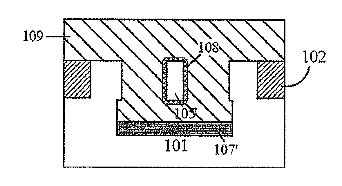
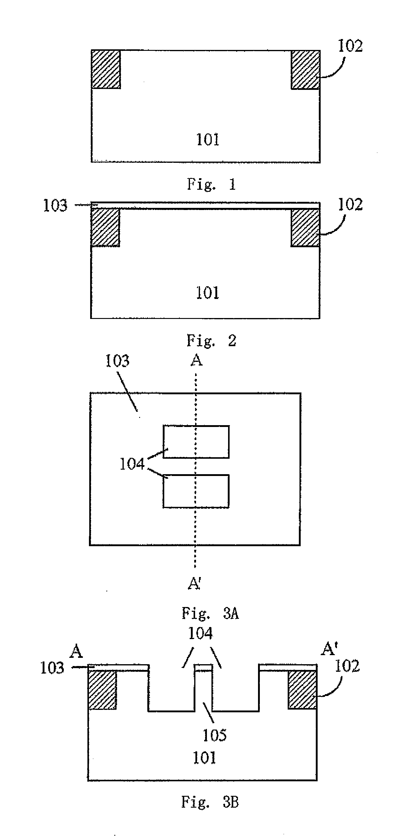
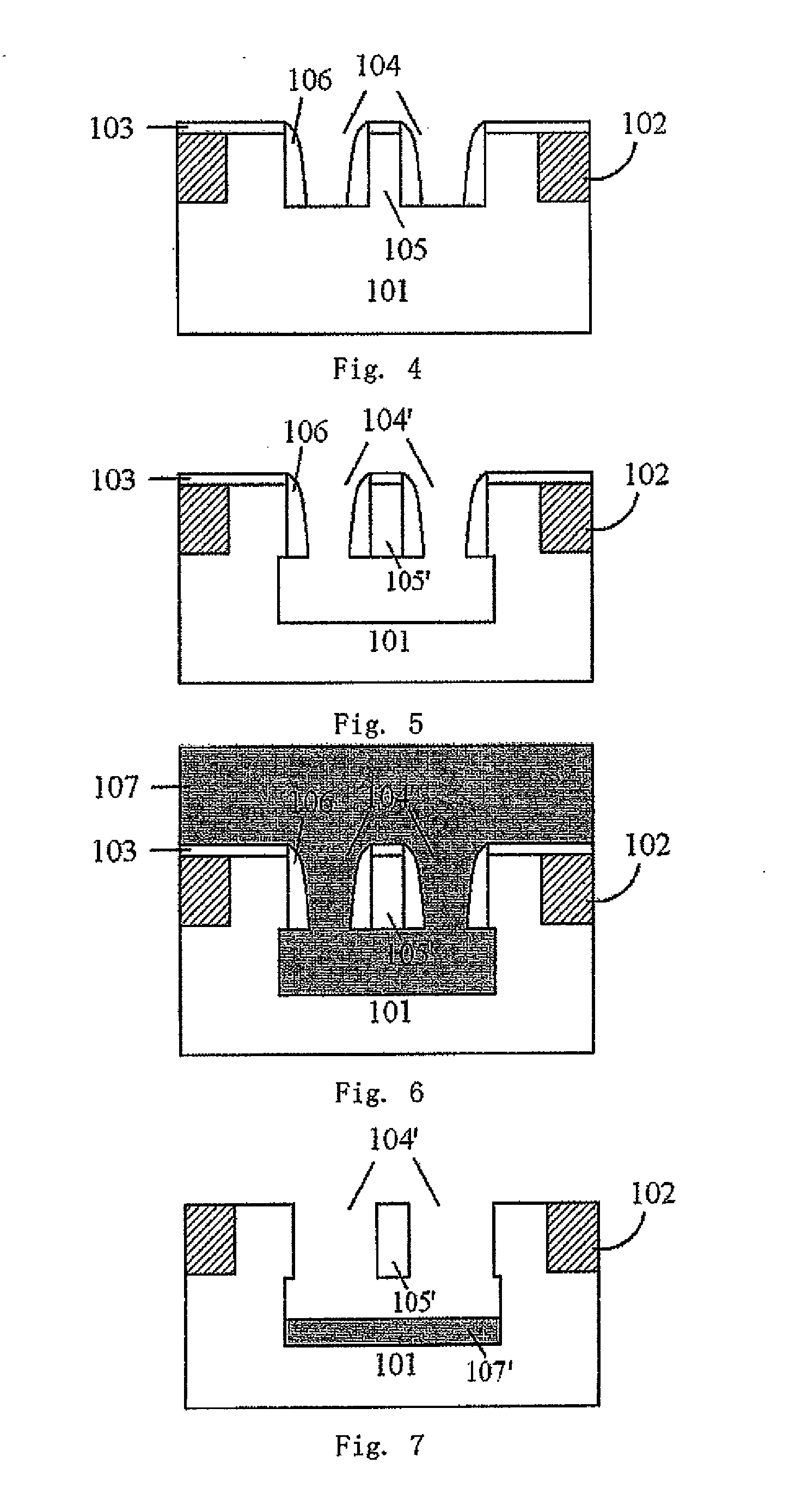
[0031]The present invention will be described below with those preferred embodiments in connection with attached drawings. However, it should be understood that the descriptions here are only illustrative, without an intend of limiting the protection scope of the present invention. Also, the following description omits details of those known structure and techniques so that concepts of the invention are not obscured unnecessarily.

[0032]Schematic layer structure according to one embodiment of the present invention is shown in the figures. However, these figures are not drawn to scale, and some details may be exaggerated and other details may be omitted for simplicity. Shapes, relative sizes and positions of various regions / layers shown in the figures are only illustrative. Variations may exist due to manufacturing tolerance and technical limitations. Moreover, those skilled in the art may design the regions / layers having different shapes, relative sizes and positions in view of actua...


PUM


Abstract

The present application discloses a method for manufacturing a gate-all-around field effect transistor, comprising the steps of forming a suspended fin in a semiconductor substrate; forming a gate stack around the fin; and forming source/drain regions in the fin on both sides of the gate stack, wherein an isolation dielectric layer is formed in a portion of the semiconductor substrate which is adjacent to bottom of both the fin and the gate stack. The present invention relates to a method for manufacturing a gate-all-around device on a bulk silicon substrate, which suppress a self-heating effect and a floating-body effect of the SOI substrate, and lower a manufacture cost. The inventive method is a conventional top-down process with respect to a reference plane, which can be implemented as a simple manufacture process, and is easy to be integrated into and compatible with a planar CMOS process. The inventive method suppresses a short channel effect and promotes miniaturization of MOSFETs.

Description

BACKGROUND OF THE INVENTION[0001]1. Field of Invention[0002]The present invention relates to semiconductor technology, and more particularly, to a method for manufacturing a suspended fin and a gate-all-around field effect transistor on a bulk silicon.[0003]2. Description of Prior Art[0004]The integrated circuit industry continues developing according to Moore's law and the feature size of CMOS devices is becoming smaller and smaller. A planar CMOS device on a bulk silicon is facing with severe challenges, such as a short channel effect (SCE), leakage current between the source and the drain, a drain induced barrier lowering effect (DIBL), and the like. To solve the above problems, many novel device structures are proposed, in which a gate structure of the device is changed from the initial single-gate structure to a double-gate structure (i.e. FinFET), a multi-gate structure, or even a surrounding gate which surrounds the channel completely. With an increase of the number of the ga...

Claims


Application Information

Patent Timeline
Patent Type & Authority Applications(United States)
IPC IPC(8): H01L21/336H01L21/302
CPCH01L29/66795H01L29/42376
Inventor ZHOU, HUAJIESONG, YIXU, QIUXIA
Owner INST OF MICROELECTRONICS CHINESE ACAD OF SCI
Why Eureka
Try Eureka