
Dynamic random access memory cell and array having vertical channel transistor

a memory cell and dynamic random access technology, applied in the field of dynamic random access memory cell arrays with vertical channel transistors, can solve the problems of short channel effect, current reduction of transistors, and inability to enhance the device performance, so as to prevent the generating of coupling noise and enhance device performan

Active Publication Date: 2012-06-21
POWERCHIP SEMICON MFG CORP
View PDF42 Cites 59 Cited by
  • Summary
  • Abstract
  • Description
  • Claims
  • Application Information

AI Technical Summary

Benefits of technology

[0010]Accordingly, the invention is directed to a dynamic random access memory cell and a dynamic random access memory cell array having vertical channel transistor which are capable of preventing the generating of coupling noise between adjacent BLs and enhancing device performance.
[0021]As the dynamic random access memory cell and dynamic random access memory cell array having vertical channel transistor of the invention have the assisted gates (assisted gate lines) disposed therein, the resistance of the embedded BLs can be controlled by applying a voltage via the assisted gates (assisted gate lines). The resistance of the embedded BLs is then lowered to enhance the operation efficiency of the device. Moreover, the height of the embedded BLs can be controlled through the height of the assisted gates (assisted gate lines).
[0022]In the dynamic random access memory cell and dynamic random access memory cell array having vertical channel transistor of the invention, as the assisted gates (assisted gate lines) are disposed between the embedded BLs, the generation of coupling noise between adjacent BLs can be prevented, thereby reducing the device size.
[0023]Additionally, the methods for fabricating the dynamic random access memory cell and dynamic random access memory cell array having vertical channel transistor of the invention are simple.

Problems solved by technology

However, this leads to problems such as severe short channel effect and on current reduction of transistors.
However, the embedded BLs formed by the doped region have higher resistance and cannot enhance the performance of devices.
The fabrication becomes more difficult when the doping concentration and doping depth are increased to lower the resistance of the embedded BLs.
However, the fabrication of the metal embedded BLs is complicated.
Moreover, when operating DRAM, severe coupling noise may be generated between two adjacent embedded BLs so as to affect the performance of devices.

Method used


Image

  • Dynamic random access memory cell and array having vertical channel transistor
  • Dynamic random access memory cell and array having vertical channel transistor
  • Dynamic random access memory cell and array having vertical channel transistor

Examples


Embodiment Construction

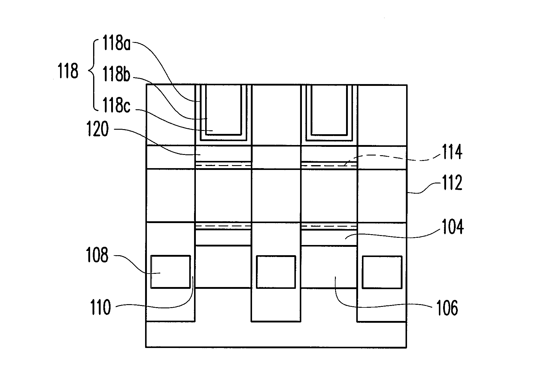
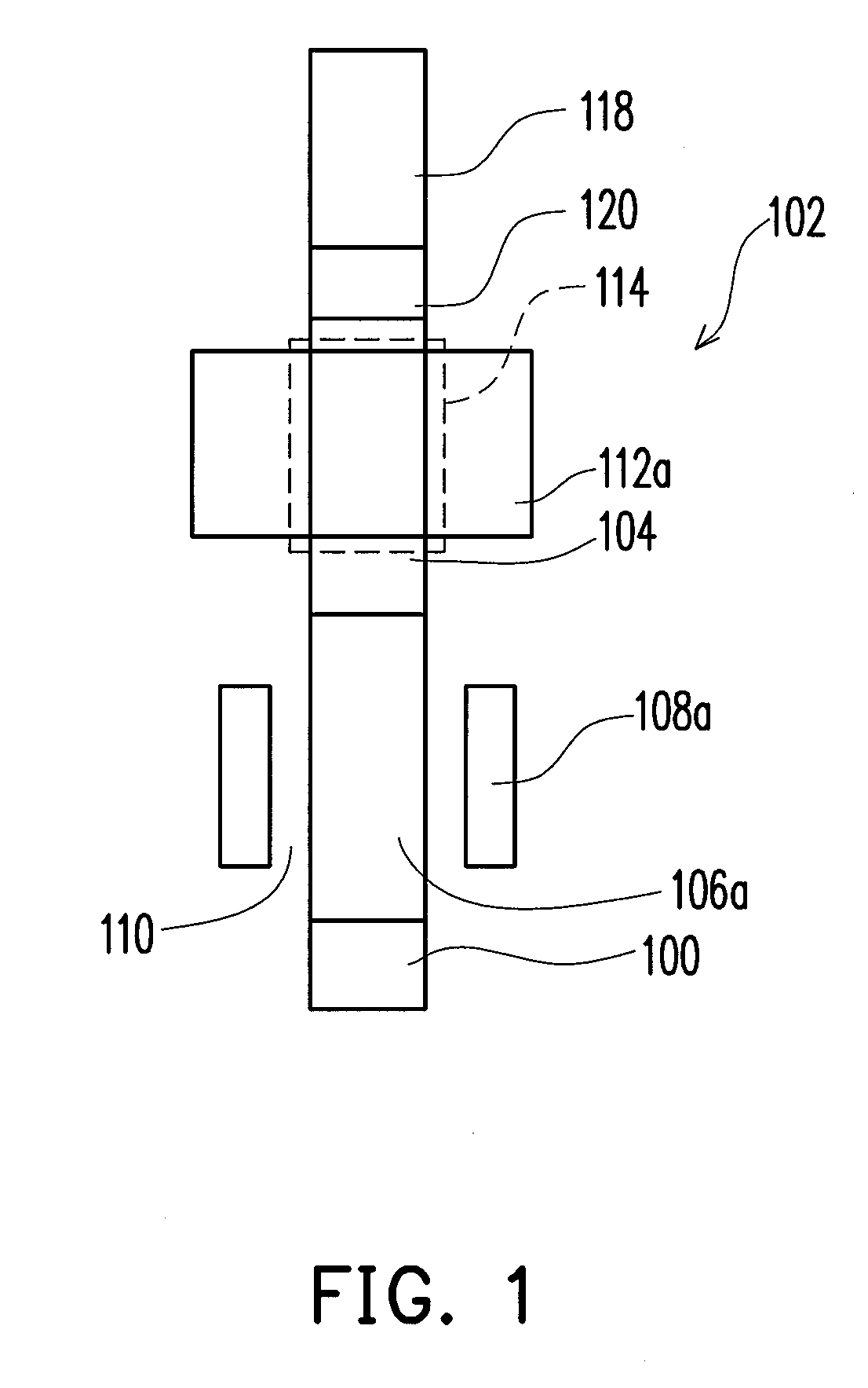
[0030]FIG. 1 illustrates a cross-sectional view of a dynamic random access memory cell having vertical channel transistor array according to an embodiment of the invention.

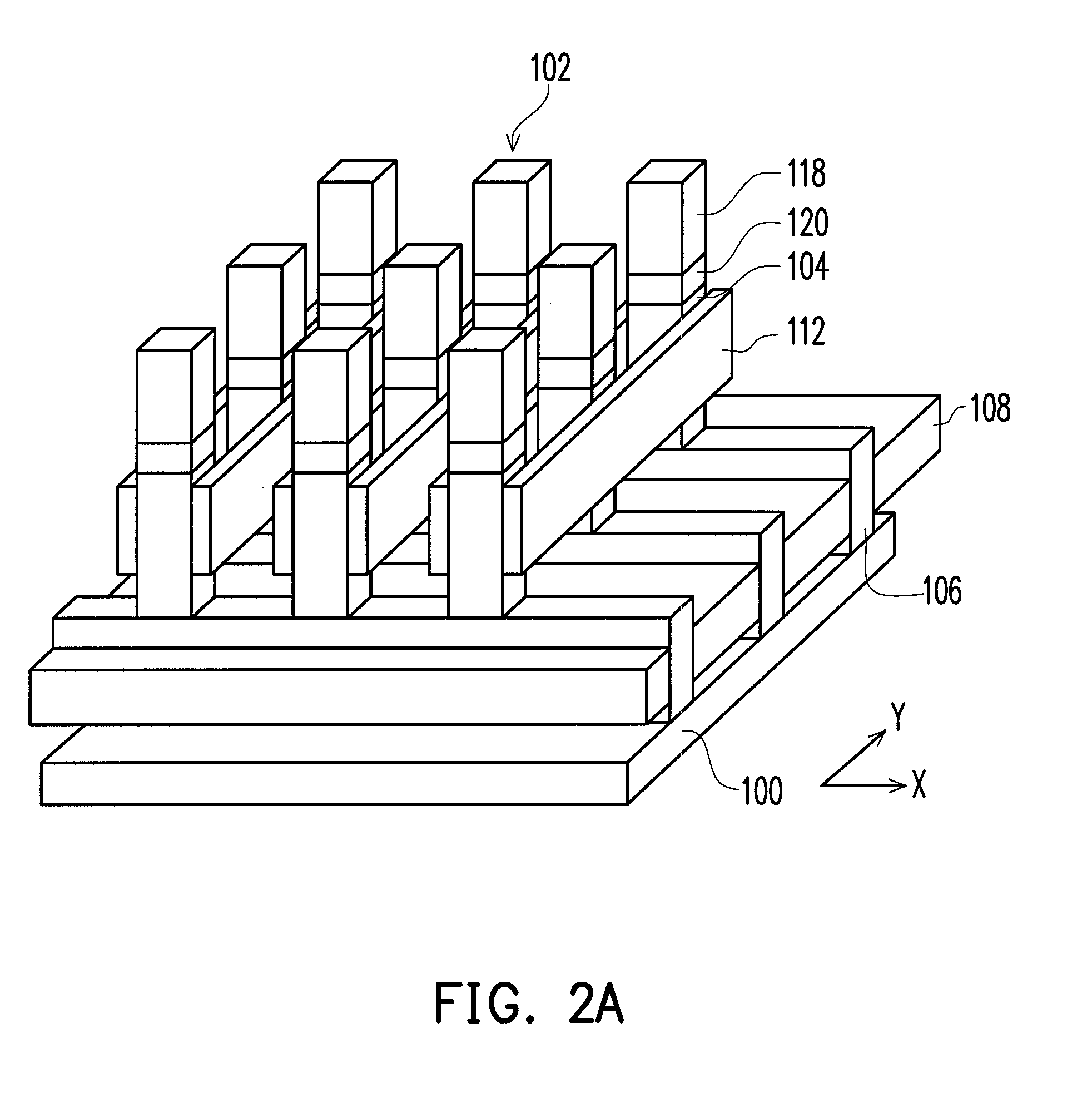
[0031]Referring to FIG. 1, a dynamic random access memory cell 102 having vertical channel transistor of the invention includes a semiconductor pillar 104, a drain layer 106a, an assisted gate 108a, a control gate 112a, a capacitor 118, and a source layer 120.

[0032]The semiconductor pillar 104 is disposed in a semiconductor substrate 100 and forms an active region of a vertical channel transistor. The semiconductor substrate 100 is, for example, a silicon substrate. The semiconductor pillar 104 is, for example, a silicon pillar.

[0033]The drain layer 106a is disposed at the bottom of the semiconductor pillar 104. The drain layer 106a is constituted by a doped region, for example. The drain layer 106a can be an N-type doped region or a P-type doped region corresponding to the type of the vertical channel transistor....


PUM


Abstract

A dynamic random access memory cell having vertical channel transistor includes a semiconductor pillar, a drain layer, an assisted gate, a control gate, a source layer, and a capacitor. The vertical channel transistor has an active region formed by the semiconductor pillar. The drain layer is formed at the bottom of the semiconductor pillar. The assisted gate is formed beside the drain layer, and separated from the drain layer by a first gate dielectric layer. The control gate is formed beside the semiconductor pillar, and separated from the active region by a second gate dielectric layer. The source layer is formed at the top of the semiconductor pillar. The capacitor is formed to electrical connect to the source layer.

Description

CROSS-REFERENCE TO RELATED APPLICATION[0001]This application claims the priority benefit of Taiwan application serial no. 99144063, filed on Dec. 15, 2010. The entirety of the above-mentioned patent application is hereby incorporated by reference herein and made a part of this specification.BACKGROUND OF THE INVENTION[0002]1. Field of the Invention[0003]The invention relates to a semiconductor device and a fabricating method thereof and more particularly to a dynamic random access memory cell and a dynamic random access memory cell array having vertical channel transistor.[0004]2. Description of Related Art[0005]With the function of computer micro-processors becomes more powerful, the number of programs and operations performed by software becomes greater. Thus, the fabrication technology of memory has become one of the most important technologies in the semiconductor industry. Dynamic random access memory (DRAM) is a volatile memory constituted by a plurality of memory cells. Each ...

Claims


Application Information

Patent Timeline
Patent Type & Authority Applications(United States)
IPC IPC(8): H01L27/108H10B12/00
CPCH01L27/10879H01L27/10826H10B12/36H10B12/056
Inventor CHEN, HUI-HUANGCHEN, CHIH-YUANYANG, SHENG-FUCHEN, CHUN-CHENG
Owner POWERCHIP SEMICON MFG CORP
Learn More