[0009]It is a still a further object of the present invention to provide a safety switch-off or optical fuse for use in a waveguide or
optical fiber, the fuse being activated, namely decreasing drastically the output
light level, by a broad range of wavelengths.
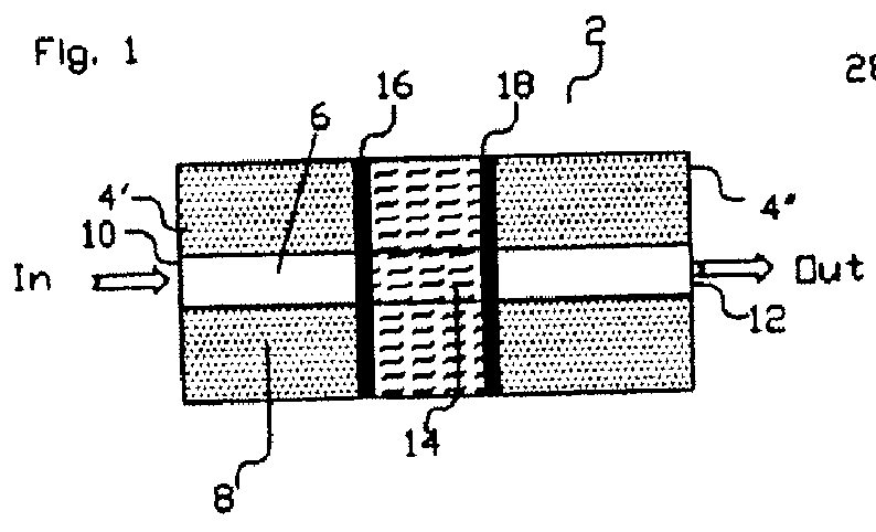
[0011]In accordance with one embodiment, there is therefore provided an optical fuse or energy-switching-off device that includes an optical waveguide having an input section and an output section, the two sections forming a pair of opposed surfaces extending transversely through the axes of the waveguide sections. A substantially transparent material disposed between the opposed surfaces comprises an
electrically conductive nanotube web immersed in
dielectric material, where the nanotubes are not in electrical contact with each other. The substantially transparent material forms a
plasma when exposed to optical signals propagating within the optical waveguide with an optical
power level above a predetermined threshold. The plasma damages the opposed surfaces sufficiently to render the surfaces substantially opaque to light propagating within the input section of the optical waveguide so as to prevent the transmission of such light.
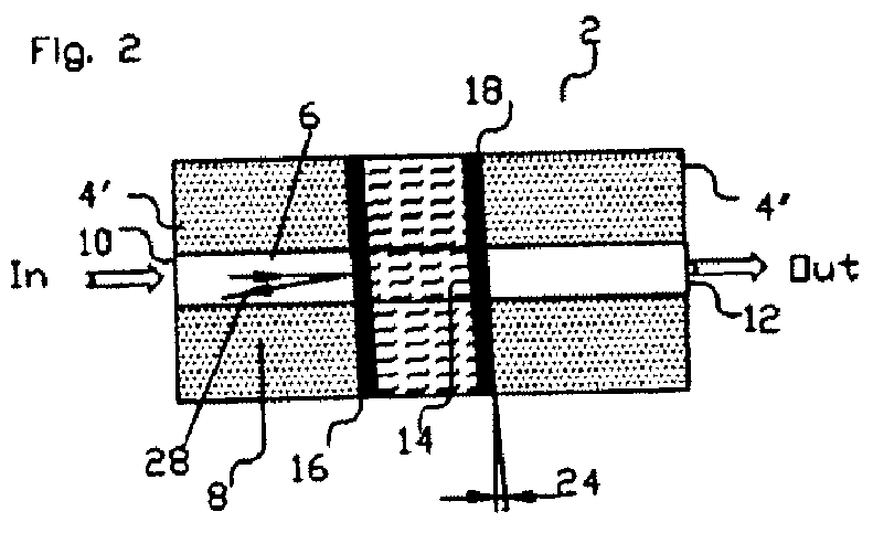
[0013]When the
thin layer is impinged with optical power exceeding a predetermined threshold, strong electric fields, which can lead to local
electrical breakdown, are generated at certain sites (“hot spots”) in proximity with the nano-web surface. This leads to a visible light emitting arc-
discharge, where plasma is created. The generated plasma greatly increases the absorption of the propagating light, and the energetic
discharge creates catastrophic damage at or near the nano-web surfaces. This damage is often seen as cratered regions. Thus, the waveguide becomes permanently highly scattering or, in other words, highly opaque for the propagating light. This significantly reduces the transmitted optical power. The
opacity is permanent, and the device acts as a fast switch for interrupting the power propagation, which occurs as fast as the breakdown is created and stays permanently as an interrupting switch due to the damage formation by the energetic breakdown. The visible light emitted by the plasma can be detected by a photo-
detector and used as an indication that the
light intensity passing through the switch is over its designed threshold.
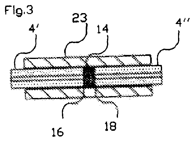
[0017]As with most
optical fiber components, minimal back reflection is desirable. This may be obtained by a combination of two methods. First, the nanotube web can be deposited at an angle, namely, not perpendicular to the direction of propagation of the light, thus preventing any back reflection from re-entering the waveguide core. This can be performed by either using an angled cleave or by using an angled fiber connector (or
ferrule). Second, the
coating dielectrics, namely glass or
polymer layers are designed to have minimal reflections, e.g., by sandwiching the nanotube web layer between two anti-reflective
layers.
[0019]In order to control the threshold power of the fuse, several methods can be used. A first method is to vary the thickness of the nanotube web layer. In general, the threshold power decreases with a thicker layer. However, in this method, the
insertion loss at the operating power also changes (the thicker the layer, the higher the loss). Thus, if one wants to keep a low
insertion loss at the operating powers, this method is rather limited in range. A second method is to use fibers of different core, or mode field diameters. A commonly used fiber in
optical communication systems is the SMF-28 single mode fiber. This fiber has a
mode field diameter of approximately 10 micrometers for 1550 nm wavelengths. Other fibers have either smaller or larger diameters. For example, High-Numerical-Aperture (HNA) fibers generally have smaller mode field diameters. Thus, in HNA fibers, the
light intensity (power per unit area) is larger than in SMF-28 fibers operating with the same power. Consequently, the power threshold in HNA fiber is lower than that in SMF-28 fibers having the same
layers. Since there are several possible HNA fibers, with different mode field diameters, one can control the threshold power using this method. Moreover, the input and output fibers can still be standard SMF-28 fibers. These are efficiently fusion spliced to the HNA fibers or other types of fibers (
insertion losses can be around 0.1 dB per splice). Thus, using different types of fibers with the same layers, can lead to switches having different thresholds and nearly the same
insertion loss at the operating powers. The same principle can be used for multi mode fibers, having various mode field diameters.
[0020]The device can be packaged in several ways. A first way is by using
optical fiber connectors. In this configuration, the device is similar (at least when viewed externally) to two pigtailed fibers, which are connected using connectors. Namely, there is an input fiber; two connectors connected using an adapter, and an output fiber. However, the difference between the fuse and the standard connector is that either one or both fibers have additional layers on their matching surfaces. A somewhat simpler configuration uses only ferrules, without the whole connector
assembly. Here, instead of two connectors and an adapter, there are two ferrules attached inside an adapter or a
mating sleeve, again, in the switching device, one or both fibers inside the ferrules have additional layers on their matching surfaces. In order to minimize reflection losses, angled ferrules or angled connectors are used.

