Semiconductor device and manufacturing method thereof

Active Publication Date: 2012-06-28
SEMICON ENERGY LAB CO LTD
View PDF12 Cites 96 Cited by
  • Summary
  • Abstract
  • Description
  • Claims
  • Application Information

AI Technical Summary

Benefits of technology

[0035]According to an embodiment of the present invention, a semiconductor device including an oxide semiconductor, which has favorable electric characteristics and is easily miniaturized, can be provided.
[0036]Further, a semiconductor device is provided in which variation in electric characteristics due to a short channel effect i

Problems solved by technology

On the other hand, although a transistor including polycrystalline silicon has high field-effect mobility, it is not suitable for being formed over a larger glass substrate.
However, in this method, argon plasma treatment is performed on the exposed surface of the oxide semiconductor; therefore, regions of the oxide semiconductor, which are to be the source region and the drain region are etched at the same time, which makes the source region and the drain region thin (see FIG. 8 in Non-Patent Do

Method used


Image

  • Semiconductor device and manufacturing method thereof
  • Semiconductor device and manufacturing method thereof
  • Semiconductor device and manufacturing method thereof

Examples


embodiment 1

[0063]In this embodiment, a transistor in which an oxide semiconductor is used for a channel and a manufacturing method thereof will be described with reference to FIGS. 1A and 1B, FIGS. 2A and 2B, FIGS. 3A to 3D, and FIGS. 4A and 4B.

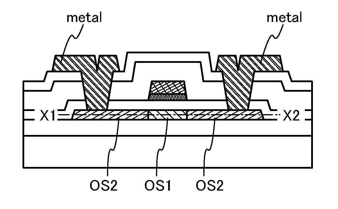
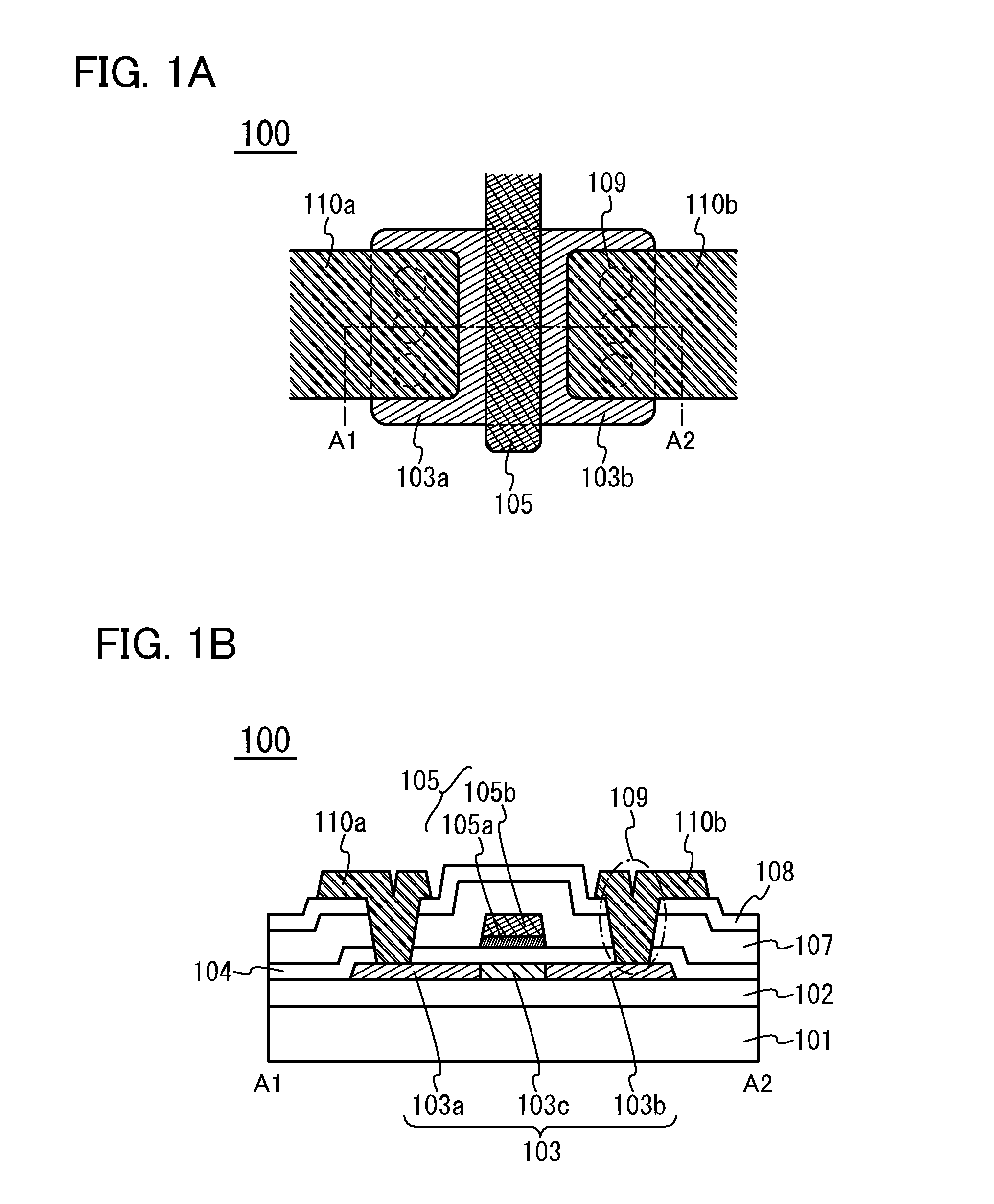
[0064]FIG. 1A is a top view illustrating a structure of a transistor 100 which is one mode of a structure of a semiconductor device, and FIG. 1B is a cross-sectional view illustrating a cross-sectional structure of a portion indicated by a chain line A1-A2 in FIG. 1A. In FIG. 1A, a substrate and an insulating layer are omitted.

[0065]In the transistor 100 illustrated in FIGS. 1A and 1B, a base layer 102 is formed over a substrate 101, and an oxide semiconductor layer 103 is formed over the base layer 102. A gate insulating layer 104 is formed over the oxide semiconductor layer 103, and a gate electrode 105 is formed over the gate insulating layer 104. An insulating layer 107 and an insulating layer 108 are formed over the gate electrode 105, and a source...

embodiment 2

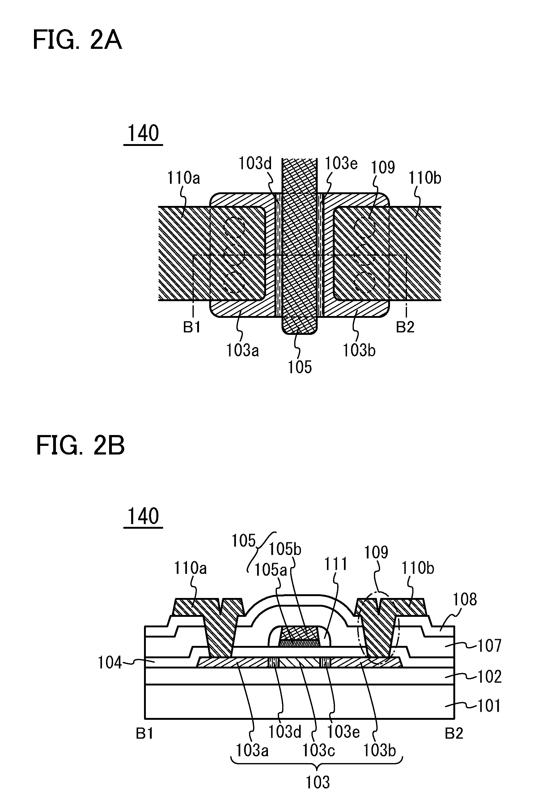
[0209]In this embodiment, examples of transistors having structures different from those of the transistors disclosed in Embodiment 1 will be described.

[0210]FIG. 5A is a top view illustrating a structure of a transistor 150 and FIG. 5B is a cross-sectional view illustrating a stacked structure of a portion indicated by a chain line C1-C2 in FIG. 5A. In FIG. 5A, a substrate and an insulating layer are omitted.

[0211]In the transistor 150 illustrated in FIG. 5B, the source electrode 110a and the drain electrode 110b are stacked in a different manner from the stacking manner of the transistor 100 disclosed in Embodiment 1. In the transistor 150, the source electrode 110a and the drain electrode 110b are formed over the base layer 102, and the oxide semiconductor layer 103 is formed over the base layer 102, the source electrode 110a, and the drain electrode 110b.

[0212]In the transistor 150, the source electrode 110a and the drain electrode 110b are connected to the source region 103a a...

embodiment 3

[0230]In this embodiment, a method for forming an oxide semiconductor film including CAAC-OS, which is different from the method disclosed in Embodiment 1, will be described.

[0231]First, an oxide semiconductor film having a thickness of greater than or equal to 1 nm and less than or equal to 50 nm is formed over the base layer 102.

[0232]The substrate temperature in deposition is set to higher than or equal to 150° C. and lower than or equal to 450° C., preferably higher than or equal to 200° C. and lower than or equal to 350° C. The deposition is performed while the substrate is heated to higher than or equal to 150° C. and lower than or equal to 450° C., preferably higher than or equal to 200° C. and lower than or equal to 350° C., whereby moisture (including hydrogen) or the like is prevented from entering a film. Further, CAAC-OS which is an oxide semiconductor layer having crystallinity can be formed.

[0233]Further, it is preferable that hydrogen be further released from the oxid...


PUM


Abstract

A semiconductor device capable of high speed operation is provided. Further, a highly reliable semiconductor device is provided. An oxide semiconductor having crystallinity is used for a semiconductor layer of a transistor. A channel formation region, a source region, and a drain region are formed in the semiconductor layer. The source region and the drain region are formed in such a manner that one or more of elements selected from rare gases and hydrogen are added to the semiconductor layer by an ion doping method or an ion implantation method with the use of a channel protective layer as a mask.

Description

BACKGROUND OF THE INVENTION[0001]1. Field of the Invention[0002]The present invention relates to a semiconductor device which includes a circuit including a semiconductor element such as a transistor, and a method for manufacturing the semiconductor device. For example, the present invention relates to an electronic device which includes, as a component, a power device mounted on a power supply circuit; a semiconductor integrated circuit including a memory, a thyristor, a converter, an image sensor, or the like; an electro-optical device typified by a liquid crystal display panel; a light-emitting display device including a light-emitting element; or the like.[0003]Note that in this specification, a semiconductor device means any device that can function by utilizing semiconductor characteristics. An electro-optical device, a light-emitting display device, a semiconductor circuit, and an electronic device are all semiconductor devices.[0004]2. Description of the Related Art[0005]A t...

Claims


Application Information

Patent Timeline
IPC IPC(8): H01L29/12H01L21/336H01L21/425H01L29/78
CPCH01L29/78693H01L29/7869H01L29/78618H01L29/78696H01L27/1225H01L27/1214H01L27/1207H01L27/1251H01L29/41733H10B12/00H01L29/66969
Inventor YAMAZAKI, SHUNPEI
Owner SEMICON ENERGY LAB CO LTD
Why Eureka
Try Eureka