Substrate processing method

a substrate processing and processing method technology, applied in the direction of electrical discharge tubes, decorative arts, electrical equipment, etc., can solve the problems of low lack of practicality of methods, and easy corrosion of substrate processing apparatus components in high temperature environments, so as to improve the etching rate of copper members and avoid vaporization

Active Publication Date: 2012-06-28
TOKYO ELECTRON LTD
View PDF3 Cites 196 Cited by
  • Summary
  • Abstract
  • Description
  • Claims
  • Application Information

AI Technical Summary

Benefits of technology

[0015]In accordance with the present disclosure, the copper member is etched by the plasma generated from the processing gas produced by adding the carbon compound gas to the hydrogen gas. Accordingly, since carbon radicals as well as the hydrogen plasma exist in the etching of the copper member, a great amount of organi

Problems solved by technology

Since, however, the halogen gas or the halogen compound gas generates strong acid, components of a substrate processing apparatus easily corrodes in the high temp

Method used


Image

  • Substrate processing method
  • Substrate processing method
  • Substrate processing method

Examples


Embodiment Construction

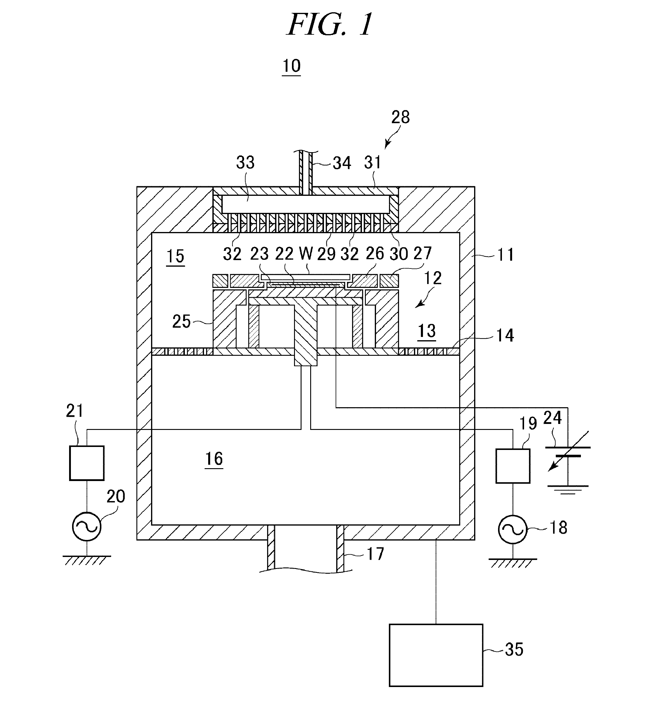
[0023]Hereinafter, illustrative embodiments of the present disclosure will be described with reference to the accompanying drawings.

[0024]FIG. 1 is a schematic configuration view of a substrate processing apparatus configured to perform a substrate processing method in accordance with an illustrative embodiment of the present disclosure. In accordance with the illustrative embodiment of the present disclosure, the substrate processing apparatus performs a plasma etching process on a wafer as a substrate for a semiconductor device (hereinafter, simply referred to as a “wafer”).

[0025]In FIG. 1, a substrate processing apparatus 10 includes a chamber 11 for accommodating therein a wafer W having a diameter of, e.g., about 300 mm. A circular column-shaped susceptor 12 for mounting thereon the wafer W is provided in the chamber 11. In this substrate processing apparatus 10, a side exhaust path 13 is formed between an inner sidewall of the chamber 11 and a side surface of the susceptor 12....


PUM

PropertyMeasurementUnit
Plasma poweraaaaaaaaaa

Abstract

There is provided a substrate processing method capable of increasing an etching rate of a copper member without using a halogen gas. A Cu layer 40 having a smoothened surface 50 is obtained, and then, a processing gas produced by adding a methane gas to a hydrogen gas is introduced into an inner space of a processing chamber 15. Plasma is generated from this processing gas. In the inner space of the processing chamber 15, there exist oxygen radicals 52 generated when an oxide layer 42 is etched, and carbon radicals 53 generated from methane. The oxygen radicals 52 and the carbon radicals 53 are compounded to generate an organic acid, and the organic acid makes a reaction with copper atoms of the Cu layer 40. As a result, a complex of the organic acid having the copper atoms is generated, and the generated organic acid complex is vaporized.

Description

CROSS-REFERENCE TO RELATED APPLICATION[0001]This application claims the benefit of Japanese Patent Application No. 2010-287595 filed on Dec. 24, 2010, and U.S. Provisional Application Ser. No. 61 / 432,772 filed on Jan. 14, 2011, the entire disclosures of which are incorporated herein by reference.FIELD OF THE INVENTION[0002]The present disclosure relates to a substrate processing method for etching copper by plasma and also relates to a storage medium.BACKGROUND OF THE INVENTION[0003]In order to etch copper (Cu) widely used as a wiring material for a semiconductor device, a halogen gas, a halogen compound gas or a gas containing an ammonia (NH3) gas or a nitrogen (N2) gas in addition to the halogen gas or the halogen compound gas have been used as a processing gas in a high temperature environment. Since, however, the halogen gas or the halogen compound gas generates strong acid, components of a substrate processing apparatus easily corrodes in the high temperature environment.[0004]...

Claims


Application Information

Patent Timeline
IPC IPC(8): H01L21/3065
CPCC23F4/00H01J37/32091H01L21/76805H01L21/02068H01L21/32136H01L21/02063H01L21/32138H01L21/3065
Inventor NISHIMURA, EIICHI
Owner TOKYO ELECTRON LTD
Why Eureka
Try Eureka