

Method of producing wire-grid polarizer and wire-grid polarizer
a technology of wire-grid polarizer and wire-grid polarizer, which is applied in the direction of polarising elements, instruments, coatings, etc., can solve the problems of high production cost of devices, increased manufacturing cost of devices, and high equipment costs used in these methods, and achieves high extinction ratio inexpensively.
- Summary
- Abstract
- Description
- Claims
- Application Information
AI Technical Summary
Benefits of technology
Problems solved by technology
Method used
Image

Examples
example 1
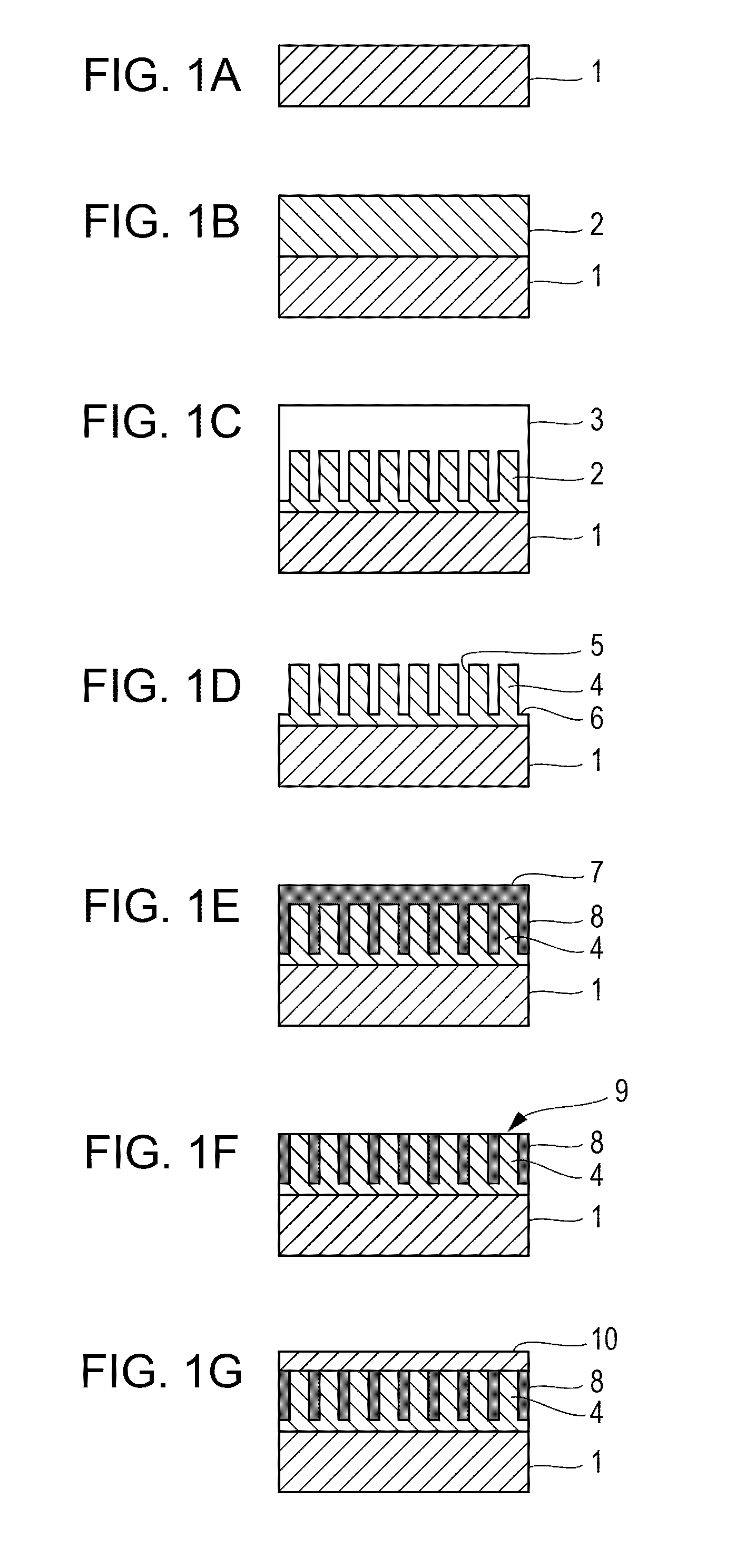
[0044]As shown in FIG. 1A, a 35 mm square glass substrate (white plate glass B-270 available from Schott AG) was washed and then dried to prepare a substrate 1. The glass transition point of the substrate is 521° C.
[0045]As shown in FIG. 1B, a sol-gel coating 2 was formed on the substrate by applying a sol-gel material containing siloxane as a main component (sol-gel coating material VRS-PRC35N-1K available from RASA Industries, Ltd.) at 1000 rpm for 30 sec with a spin coater.
[0046]As shown in FIG. 1C, the substrate 1 provided with the sol-gel coating was placed on a hot plate, a 30 mm square nickel mold 3 having a line-and-space structure on the entire one surface thereof was pressed onto the sol-gel coating, and in this state, the hot plate was heated to 200° C., maintained at the same temperature for 5 min, and then cooled to room temperature. The nickel mold 3 has a rectangular shape with a line width of 31 nm, a space width of 109 nm, and a space depth of 240 nm.
[0047]As shown ...
example 2
[0054]In the step shown in FIG. 1A, a glass substrate (optical glass L-PHL1) was used as the substrate 1. This glass substrate had a glass transition point of 347° C. In the step shown in FIG. 1B, a sol-gel coating 2 was formed on the substrate by applying a sol-gel material (sol-gel coating material VRS-PRC35N-1K available from RASA Industries, Ltd.) at 1500 rpm for 30 sec with a spin coater.
[0055]In the step shown in FIG. 1C, a nickel mold 3 having a line width of 46 nm, a space width of 94 nm, and a space depth of 200 nm was used.
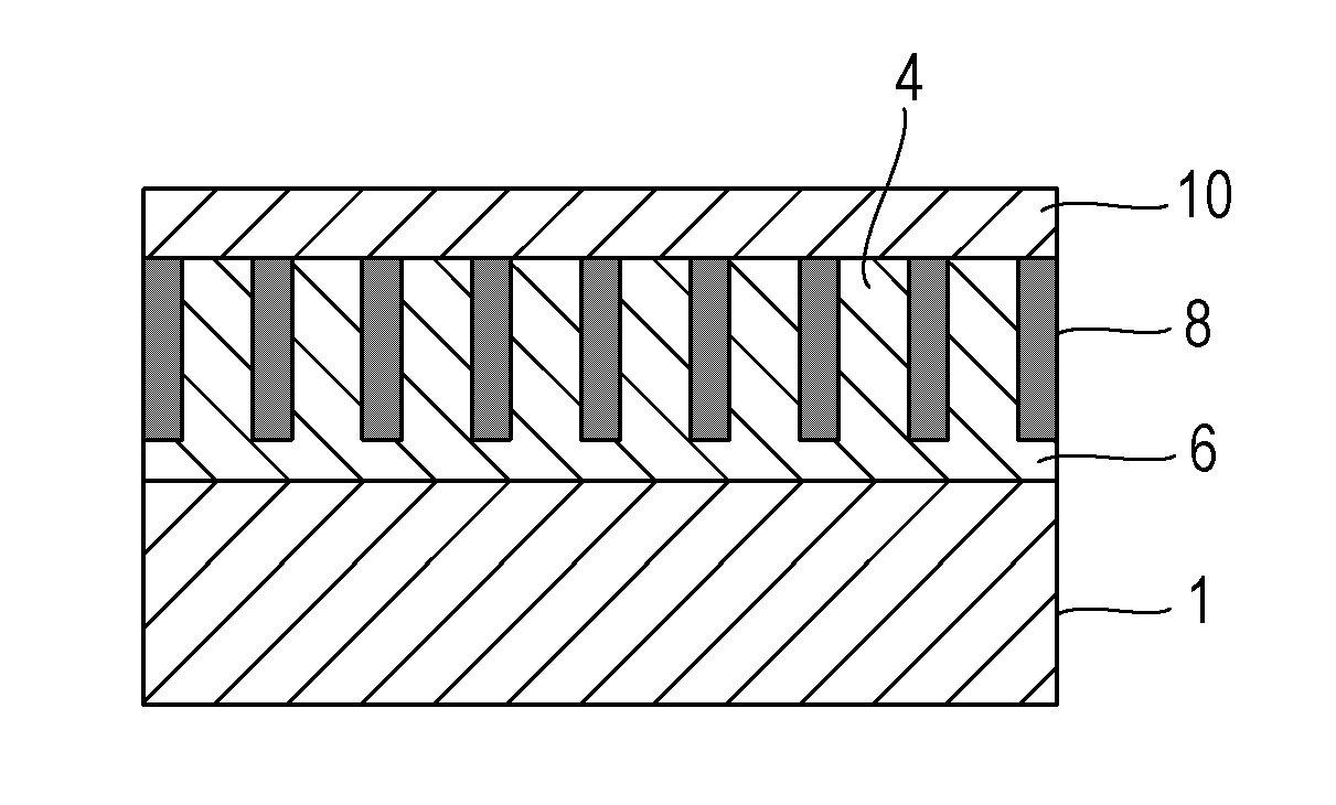
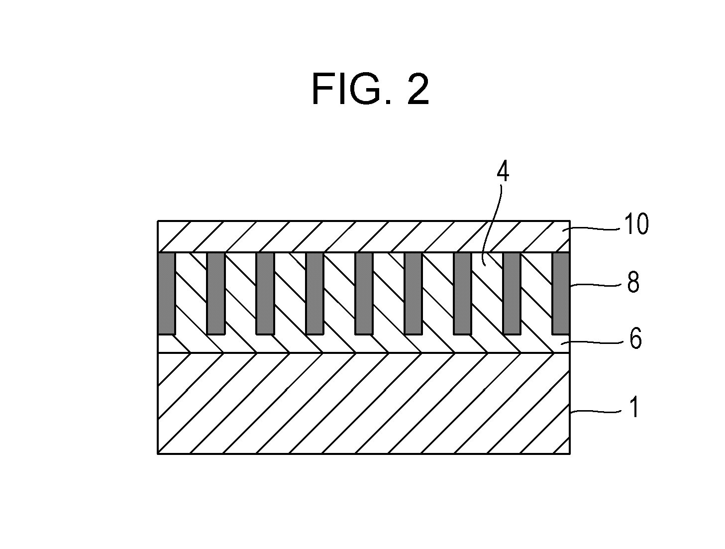
[0056]In the step shown in FIG. 1D, the mold 3 was detached, and curing was performed at 300° C. for 30 min to obtain a line-and-space transferred substrate having a structure where a line part 4 and a space part 5 are alternately and repeatedly arranged. The obtained line-and-space structure had a line width of 85 nm, a space width of 55 nm, and a space depth of 180 nm. The remaining coating part 6 had a thickness of 10 nm. Similarly, a sol-gel coating ...
example 3
[0060]In this example, a quartz substrate was used as the substrate 1 in Example 1. The nickel mold 3 used in the step in FIG. 1C had a line width of 31 nm, a space width of 109 nm, and a space depth of 222 nm.
[0061]In the step shown in FIG. 1D, the mold 3 was detached, and curing was performed in a nitrogen atmosphere at 650° C. for 30 min to obtain a line-and-space transferred substrate having a structure where a line part 4 and a space part 5 are alternately and repeatedly arranged. The obtained line-and-space structure had a line width of 94 nm, a space width of 46 nm, and a space depth of 200 nm. The remaining coating part 6 had a thickness of 25 nm. Similarly, a sol-gel coating was applied to another substrate and was cured at 650° C. for 30 min to obtain a coating. The refractive index of the coating was 1.31.
[0062]In the step shown in FIG. 1E, embedded metal parts 8 of Al (11% by weight)+In (89% by weight) were formed. A lump of the metal started to melt at 635° C. The space...
PUM
| Property | Measurement | Unit |
|---|---|---|
| Temperature | aaaaa | aaaaa |
| Melting point | aaaaa | aaaaa |
| Nanoscale particle size | aaaaa | aaaaa |
Abstract
Description
Claims
Application Information