

Oxide semiconductor element and semiconductor device
a technology of semiconductor elements and semiconductor devices, applied in the direction of semiconductor devices, electrical devices, transistors, etc., to achieve the effect of high speed and high mobility
- Summary
- Abstract
- Description
- Claims
- Application Information
AI Technical Summary
Benefits of technology
Problems solved by technology
Method used
Image

Examples
embodiment 1
[0052]In this embodiment, a method for manufacturing an oxide semiconductor element according to one embodiment of the disclosed invention will be described with reference to FIGS. 1A and 1B, FIGS. 2A to 2E, and FIGS. 3A to 3D.
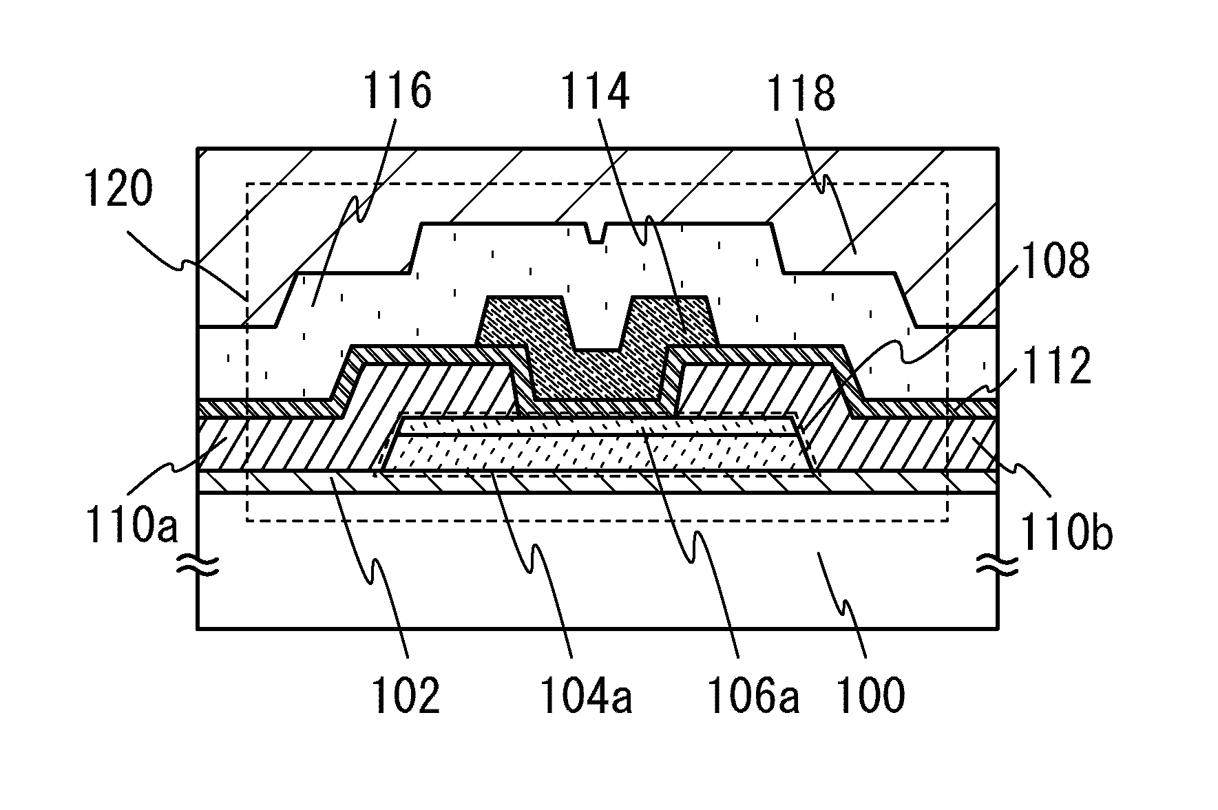
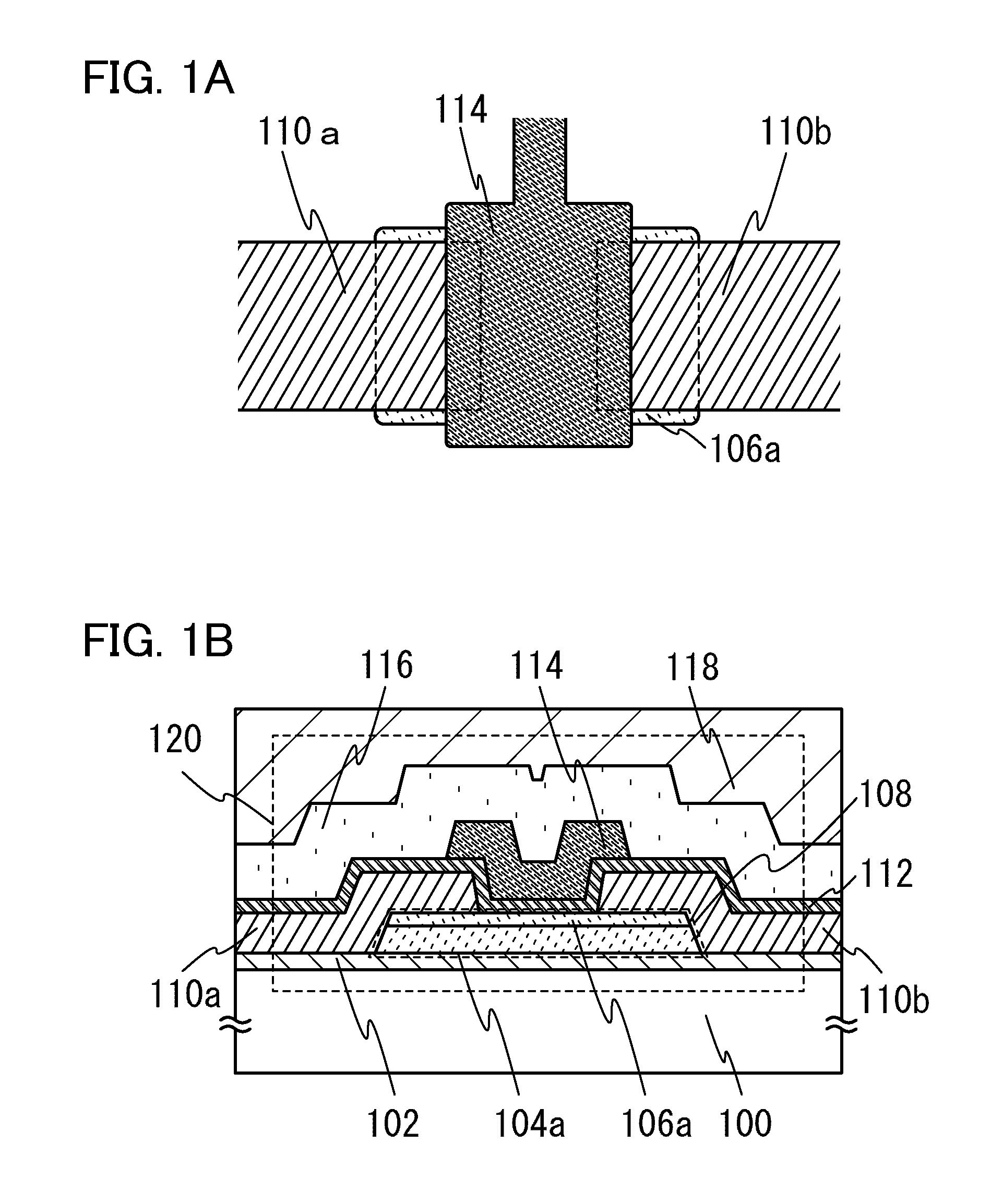
[0053]FIGS. 1A and 1B are views illustrating a top-gate transistor 120 which is an example of a structure of a semiconductor device manufactured by a method in this embodiment. FIGS. 1A and 1B are a top view and a cross-sectional view of the transistor 120, respectively. Note that some components (a substrate 100, for example) are omitted in FIG. 1A to avoid complication. Although a method for manufacturing an n-channel transistor whose carriers are electrons will be described as the transistor 120 in this embodiment, the transistor 120 is not limited to the n-channel transistor.
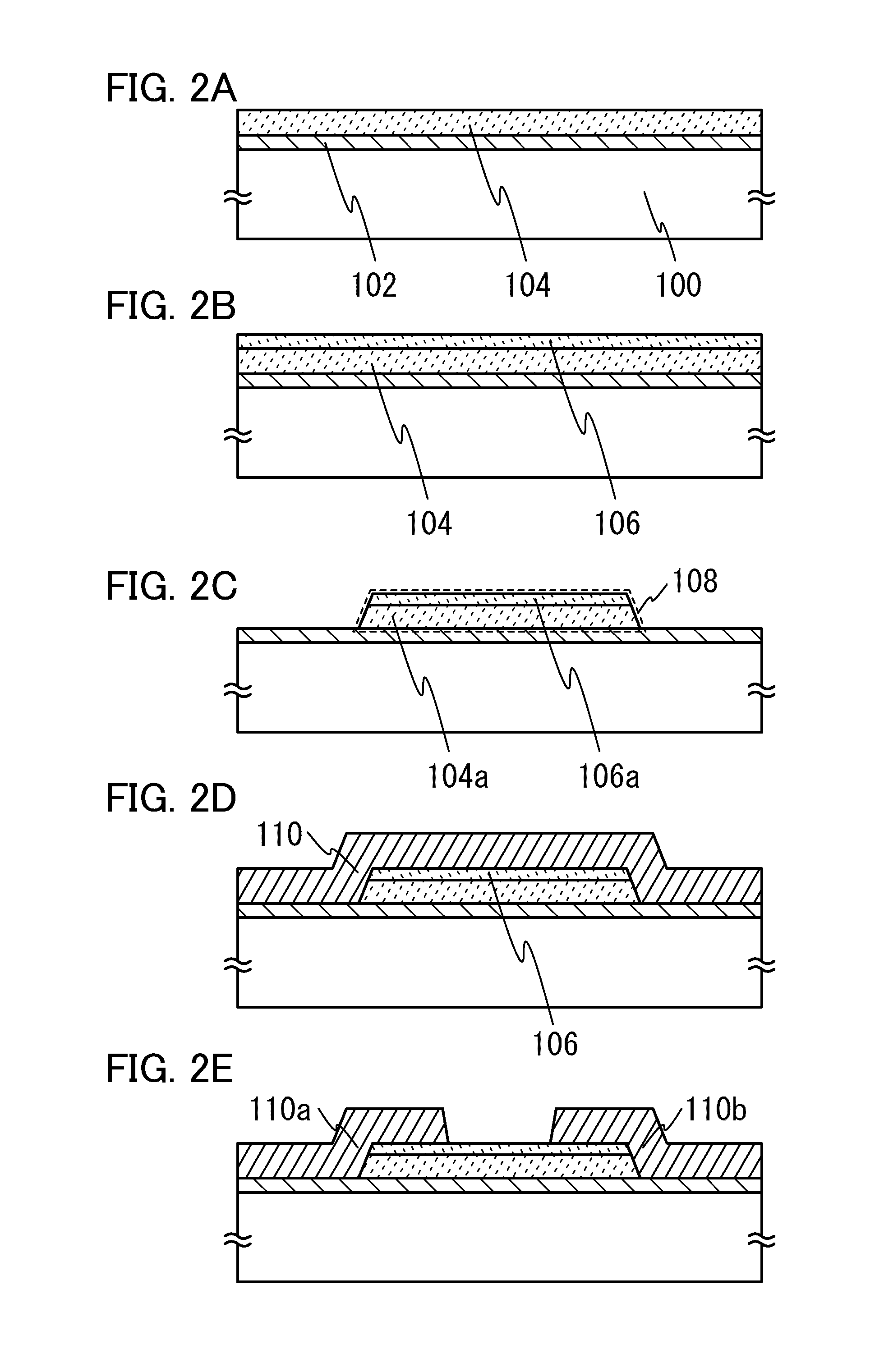
[0054]A method for manufacturing the transistor 120 will be described below with reference to FIGS. 2A to 2E and FIGS. 3A to 3D.
[0055]First, an insulating layer 102 is formed over the ...
embodiment 2
[0138]In this embodiment, a method for forming the oxide semiconductor layer 108, which is different from that described in Embodiment 1, will be described with reference to FIGS. 4A to 4C.
108 in Embodiment 2>
[0139]First, the insulating layer 102 is formed over the substrate 100, the first oxide semiconductor film 104 is deposited over the insulating layer 102, and a region including at least a surface of the first oxide semiconductor film 104 is crystallized by the first heat treatment (see FIG. 4A). FIG. 4A corresponds to FIG. 2A in Embodiment 1. Since the steps up to here are similar to that of Embodiment 1, the description is omitted here.
[0140]Next, impurity addition treatment 405 is performed on the first oxide semiconductor film 104 (see FIG. 4B), so that a region to which an impurity is added, which functions as the second oxide semiconductor film 106, is formed in the first oxide semiconductor film 104 from a surface (surface over which the gate insulating layer 112 is form...
embodiment 3
[0145]In this embodiment, a method for forming the oxide semiconductor layer 108, which is different from that described in Embodiment 1, will be described with reference to FIGS. 5A to 5C.
108 in Embodiment 3>
[0146]First, the insulating layer 102 is formed over the substrate 100, the second oxide semiconductor film 106 is deposited over the insulating layer 102, and the second oxide semiconductor film 106 is crystallized by the second heat treatment (see FIG. 5A). Note that deposition conditions, materials, processing methods, and the like used for components denoted by the same reference numerals as those in Embodiment 1 are the same as those in Embodiment 1. Therefore, description thereof is omitted here.
[0147]Next, the impurity addition treatment 505 is performed on the second oxide semiconductor film 106 (see FIG. 5B), so that a region to which an impurity is added, which functions as the first oxide semiconductor film 104, is formed in the second oxide semiconductor film 106 fr...
PUM
 Abstract
Description
Claims
Application Information