Wide-band-gap reverse-blocking MOS-type semiconductor device

a technology of mos-type semiconductor and wide-band gap, which is applied in the direction of semiconductor devices, semiconductor/solid-state device details, electrical apparatus, etc., can solve the problems of difficult sic power devices and gan power devices, troublesome inverter/converter combination life, etc., and achieve reliable reverse blocking capability and facilitate current making

Inactive Publication Date: 2012-08-23
FUJI ELECTRIC CO LTD
View PDF3 Cites 26 Cited by
  • Summary
  • Abstract
  • Description
  • Claims
  • Application Information

AI Technical Summary

Benefits of technology

[0039]The wide-band-gap reverse-blocking MOS-type semiconductor device according to embodiments of the invention, which employs a wide-band-gap semiconductor material such as SiC and GaN for the main substrate material, facilitates making a current, high enough for the power device, flow with a low ON-voltage and exhibits a very reliable reverse blocking capability.

Problems solved by technology

Since the inverter / converter combination uses an electrolytic capacitor for the interposed capacitor, it has been troublesome for the life of the inverter / converter combination to be determined by the life of the electrolytic capacitor.
Therefore, it is hard for the SiC power device and the GaN power device of the 600 V breakdown voltage class or of the 1200 V breakdown voltage class to turn the low ON-voltage to the advantage thereof.
However, the GaN MOSFET described in the Patent Document 3 is not a MOSFET that exhibits a reverse blocking capability.

Method used


Image

  • Wide-band-gap reverse-blocking MOS-type semiconductor device
  • Wide-band-gap reverse-blocking MOS-type semiconductor device
  • Wide-band-gap reverse-blocking MOS-type semiconductor device

Examples


Embodiment Construction

[0059]Now embodiments of the invention will be described in detail hereinafter with reference to the accompanied drawings which illustrate the preferred embodiments of the invention.

[0060]Although the invention is described in connection with embodiments thereof, changes and modifications are obvious to the persons skilled in the art without departing from the true spirit of the invention. Therefore, the invention is to be understood not by the specific descriptions herein but by the appended claims thereof.

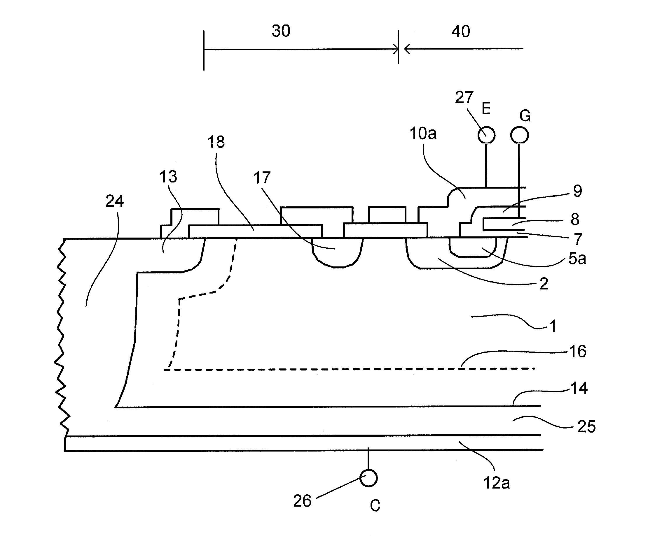
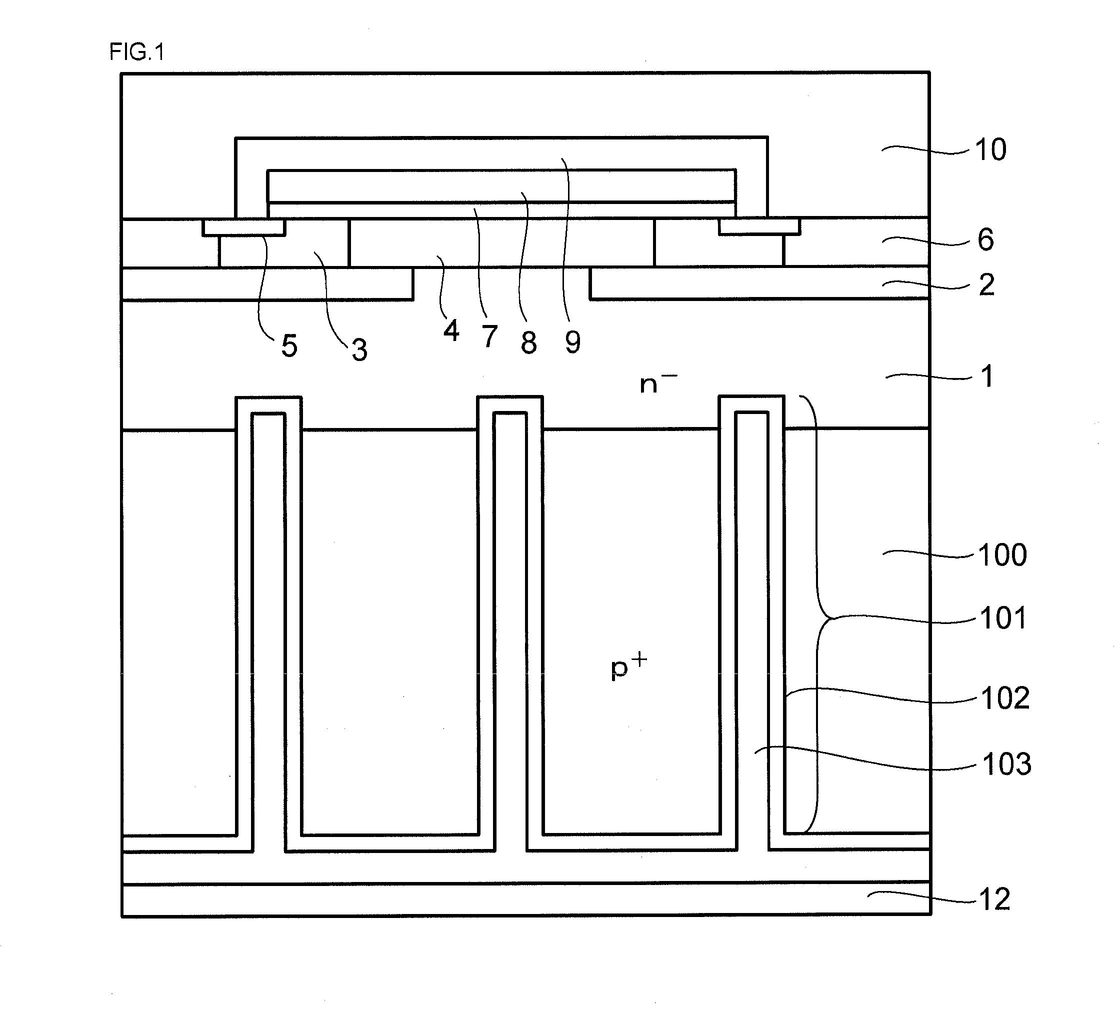
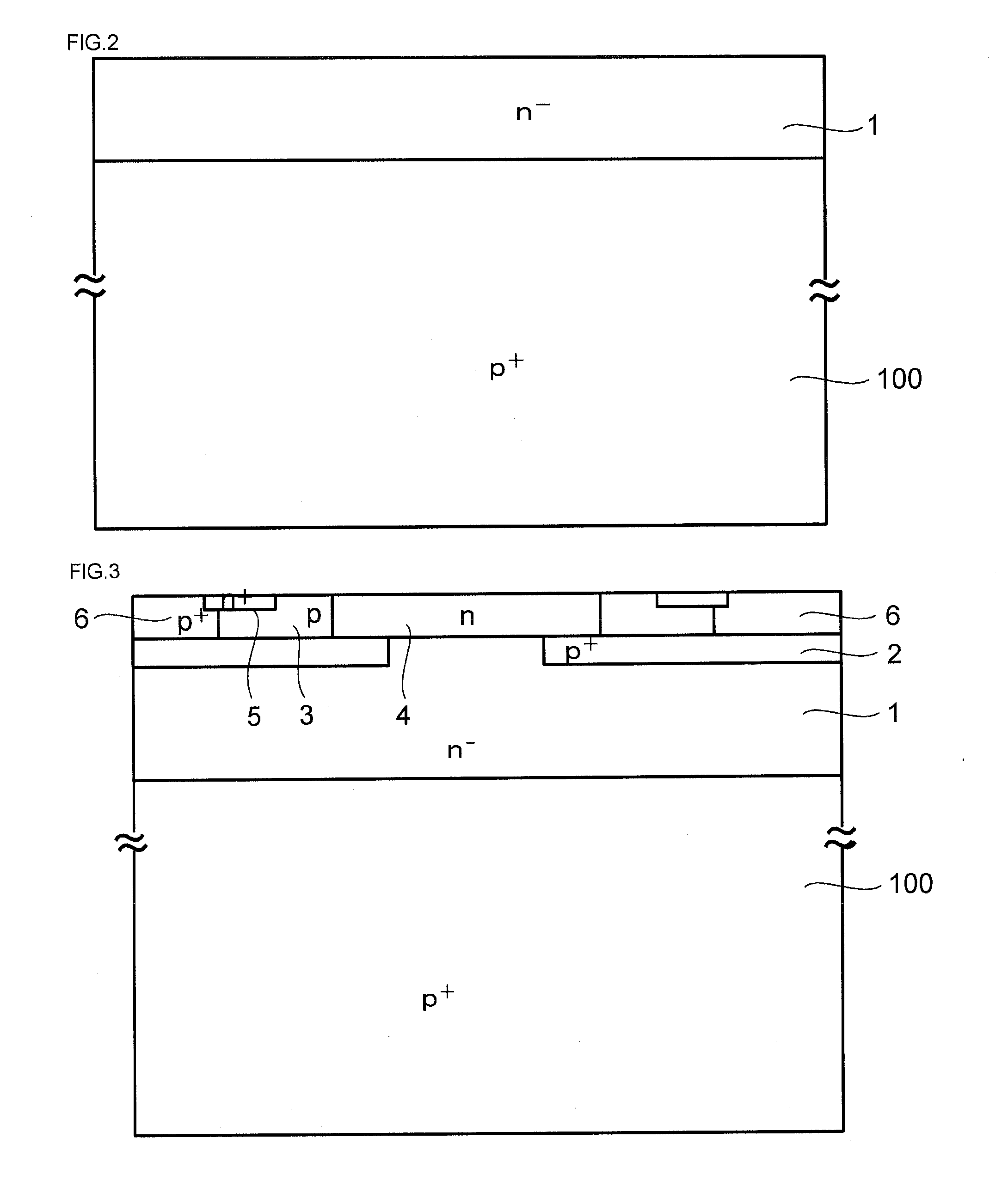
[0061]FIG. 1 is the cross sectional view of a SiC reverse-blocking MOSFET according to a first embodiment of the invention.

[0062]As shown in FIG. 1, the SiC reverse-blocking MOSFET according to the first embodiment includes p+-type SiC substrate 100 and n−-type SiC layer 1 doped more lightly than substrate 100 and formed on one major surface of substrate 100. In the surface portion of n−-type SiC layer 1, a MOS-gate structure described later is formed. Above the MOS-gate structur...


PUM


Abstract

A wide-band-gap reverse-blocking MOS-type semiconductor device includes a SiC n−-type drift layer; a p+-type substrate on the first major surface side of the drift layer; a trench extending through a p+-type substrate into the drift layer; a titanium electrode in the trench bottom that forms a Schottky junction with the SiC n−-type drift layer; an active section including a MOS-gate structure on the second major surface side of the drift layer facing to the area, in which the Schottky junctions are formed; a breakdown withstanding section surrounding the active section; and a trench isolation layer surrounding the breakdown withstanding section, the trench isolation layer extending from the second major surface of the drift layer into p+-type substrate and including insulator film buried therein. The device facilitates making a high current flow with a low ON-voltage and exhibits a very reliable reverse blocking capability.

Description

CROSS-REFERENCE TO RELATED APPLICATIONS[0001]This application claims the benefit under 35 U.S.C. §119 to Japanese Application No. 2011-034298, filed Feb. 21, 2011, in the Japanese Intellectual Property Office, the content of which is incorporated herein by reference.BACKGROUND[0002]1. Field[0003]Embodiments of the present invention relate to wide-band-gap reverse-blocking MOS-type semiconductor devices which control a high current and a high voltage. Specifically, embodiments of the invention relate to wide-band-gap reverse-blocking MOS-type semiconductor devices which facilitate securing a predetermined breakdown voltage, even if a reverse voltage is applied between the drain and source thereof.[0004]2. Description of the Related Art[0005]Recently, the use of two-way switching devices for matrix converters such as direct-link-type converter circuits has been attracting much attention from the view points of reducing the size thereof, reducing the weight thereof, improving the effic...

Claims


Application Information

Patent Timeline
Patent Type & Authority Applications(United States)
IPC IPC(8): H01L29/161
CPCH01L29/0615H01L29/0653H01L2924/0002H01L29/0657H01L29/0661H01L29/0834H01L29/0847H01L29/1095H01L29/1608H01L29/41741H01L29/41766H01L29/45H01L29/47H01L29/66068H01L29/7395H01L2924/00
Inventor YOSHIKAWA, KOH
Owner FUJI ELECTRIC CO LTD
Why Eureka
Try Eureka