[0010]Advantageously, a method that can be carried out easily is provided by means of the invention with which the shape and / or size of an
electrically conductive metal film inside a carrier is changed to targetedly adapt the metal film to a predetermined function, for example as an
electrode or
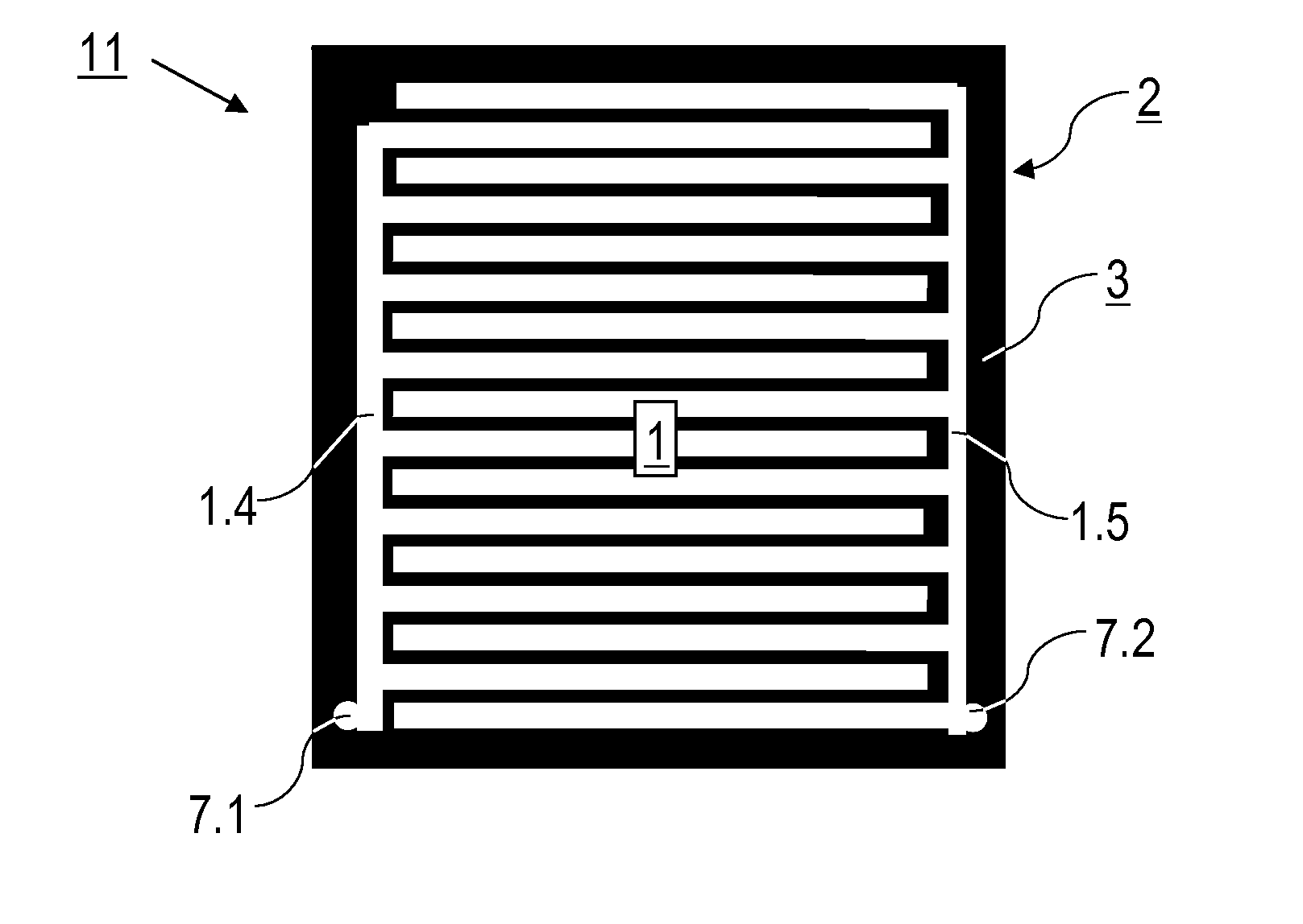
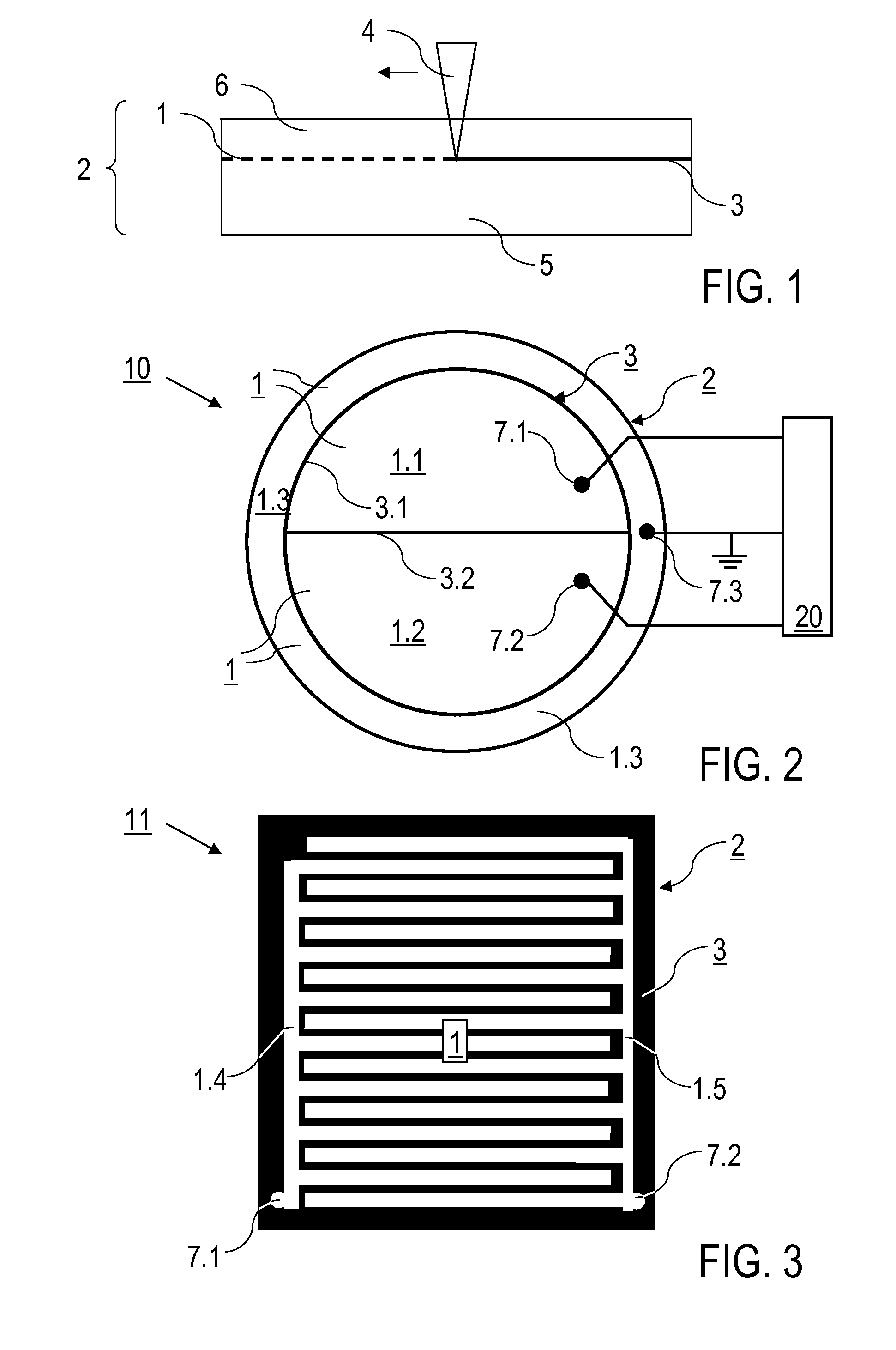
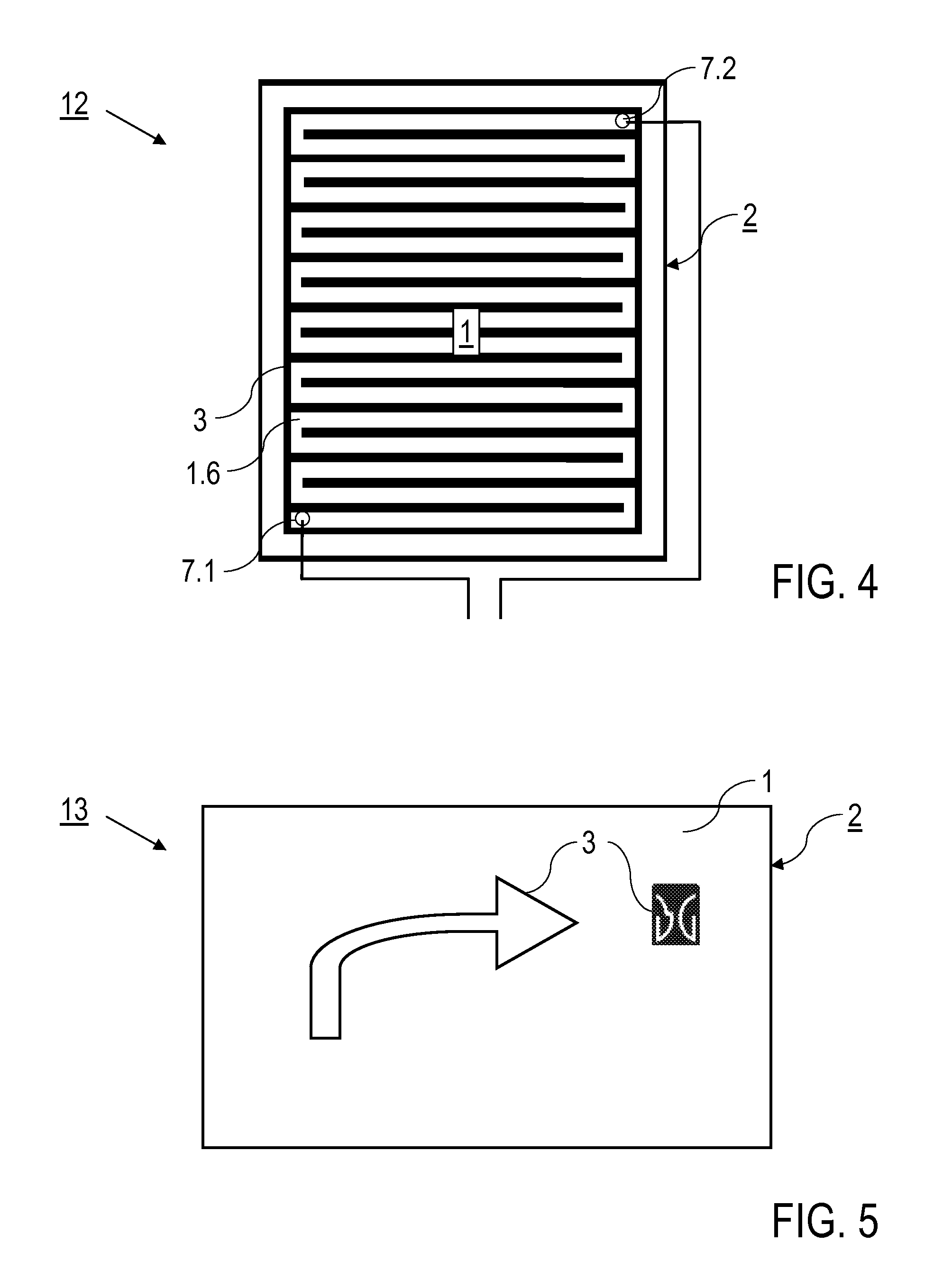
resistor element. Alternatively, the processing of the metal film can be performed with the purpose to form the at least one insulator section in a predetermined shape. The inventors have found that the optical, visually perceptible properties of the at least one insulator section differ from those of the metal film. While a metal film is highly reflective, for example, the at least one insulator section may be absorbent (in particular dark or black), transparent or opaque, for example. This property allows for the generation of a predetermined, visually perceptible pattern, such as, for example, a picture or graphic symbols, in particular writing, by processing the metal film in the carrier. According to another alternative, the at least one insulator section can be formed to electrically insulate a part of the metal film, for example a defective part of an
electrode, from the remaining metal film.
[0012]The implementation of the invention is advantageously not limited to certain materials or dimensions of the metal film. The term “metal film” is used to refer to any film (layer) of an
electrically conductive substance consisting of a metal or including a metal. The invention is preferably implemented with a thin film made of metal as in this case, the transformation of the metal film in the insulator section over the entire thickness of the metal film is facilitated. To this end, the metal film preferably has a thickness that is less than 0.5 μm, particularly preferably less than 0.25 μm. To ensure the function of the metal film in the carrier, for example as an electrode or heating
resistor, the metal film preferably features a thickness that is at least 100 nm, preferably at least 250 nm. The term “carrier” is used to refer to any
solid and high-melting material (
melting point above 500° C.) which is insusceptible to the short-term increase in temperature to transform the metal film into the at least one insulator section and is preferably electrically insulating. The carrier can be formed in one piece from a single material or in several pieces, in particular in several
layers from carrier elements, all of which consisting of a common material or of different materials. The metal film is embedded in the carrier, i.e. arranged in the carrier in such a way that the metal film is limited on both sides along its planar expansion by the carrier. The depth of the embedding in the carrier, in particular the thickness of the carrier elements, is preferably at least 100 μm and / or preferably not more than 10 mm, in particular not more than 5 mm. Preferably, the carrier has likewise a laminar (planar) expansion, for example in the shape of a flat or curved plate.
[0013]According to a preferred embodiment of the invention, the metal film is locally heated using
laser radiation to transform the metal film into an insulator at the site of the
irradiation with the laser radiation. In order to achieve at least one insulator section with a linear or planar expansion, the
irradiation can be repeated along the desired line or area of the at least one insulator section. The heating of the metal film using laser radiation has the following advantages.
[0014]Firstly, the increase in temperature can be limited to the metal film. To this end, laser radiation having a
wavelength, which is absorbed by the metal film and at which the carrier is transparent is preferably used. The
wavelength of the laser radiation is typically chosen from the
ultraviolet, visible or
infrared spectral region, while the carrier is at least on that side from which the laser radiation is directed onto the metal film for laser radiation of the chosen
wavelength transparent. Secondly, the laser radiation makes local heating of the metal film possible. The transformation of the metal film into the insulator section is in each case limited to the
irradiation site and is possible without a detrimental damage of the embedding material such that the surrounding materials of the carrier and the adjacent metal film remain virtually unaffected. Undesirable changes of the carrier, such as, for example, thermally induced distortions, can be avoided. Furthermore, the locally acting laser radiation makes processing the metal film with a
high spatial resolution possible. This is particularly advantageous for the structuring of electrodes. Thirdly, the laser radiation provides the opportunity to set or change the at least one irradiation site on the metal film in a simple manner. In order to form a linear or planar insulator section, for example, it is provided for moving the
optical path of the laser radiation and the carrier with the metal film relative to one another to transform the metal film into the at least one insulator section along a line or area. The
optical path of the laser radiation can be moved relative to the carrier using movable deflection
optics, or the carrier can be moved relative to the
optical path of the laser radiation by a
mechanical drive.
[0015]The laser radiation can be focused onto the metal film. The focused irradiation can have advantages with regard to the setting of a particularly high transformation temperature and the formation of the insulator section with a
high spatial resolution. Alternatively, an unfocused irradiation can be provided. If the intensity of the laser radiation is sufficiently high to achieve the desired transformation temperature, in this case, a larger insulator section can be formed in comparison to the focused irradiation. In order to form a strip-shaped insulator section with a certain strip width, an irradiation field with a
diameter equal to the desired irradiation width can be generated by defocusing.
[0017]Studies carried out by the inventors have shown that the section of the metal film which is transformed by the increase in temperature is electrically insulating.
Metal within the metal film is at least partially oxidized by the increase in temperature, in particular under the action of the laser radiation to form the insulator section. The
oxygen required for the oxidation can be contained in the metal film. However, the carrier into which the metal film is embedded preferably comprises a material containing
oxygen, such as, for example, an
inorganic oxide compound. Advantageously, the provision of
oxygen for the transformation of the metal film is thus facilitated.


