Semiconductor device and method for manufacturing the same

a semiconductor film and semiconductor technology, applied in the direction of semiconductor devices, electrical devices, transistors, etc., can solve the problems of difficult to remove hydrogen, difficult to control the threshold voltage, and inconvenient formation over a larger glass substrate, etc., to achieve high-reliability semiconductor devices, reduce the concentration of hydrogen near the interface of oxide semiconductor films, and stable electric characteristics

Active Publication Date: 2012-09-27
SEMICON ENERGY LAB CO LTD
View PDF48 Cites 30 Cited by
  • Summary
  • Abstract
  • Description
  • Claims
  • Application Information

AI Technical Summary

Benefits of technology

[0012]An object of one embodiment of the present invention is to manufacture a highly reliable semiconductor device by giving stable electric characteristics to a transistor including an oxide semiconductor film.
[0015]Note that the hydrogen concentration in the vicinity of the interface of the oxide semiconductor film can be reduced by providing the hydrogen permeable film between the oxide semiconductor film and the hydrogen capture film.
[0016]A highly reliable semiconductor device can be manufactured by giving stable electric characteristics to a transistor including an oxide semiconductor film.

Problems solved by technology

On the other hand, although transistors formed using polycrystalline silicon have high field-effect mobility, they are not suitable for being formed over a larger glass substrate.
It is difficult to remove hydrogen in the oxide semiconductor completely; therefore, it is also difficult to control the threshold voltage.

Method used


Image

  • Semiconductor device and method for manufacturing the same
  • Semiconductor device and method for manufacturing the same
  • Semiconductor device and method for manufacturing the same

Examples


embodiment 1

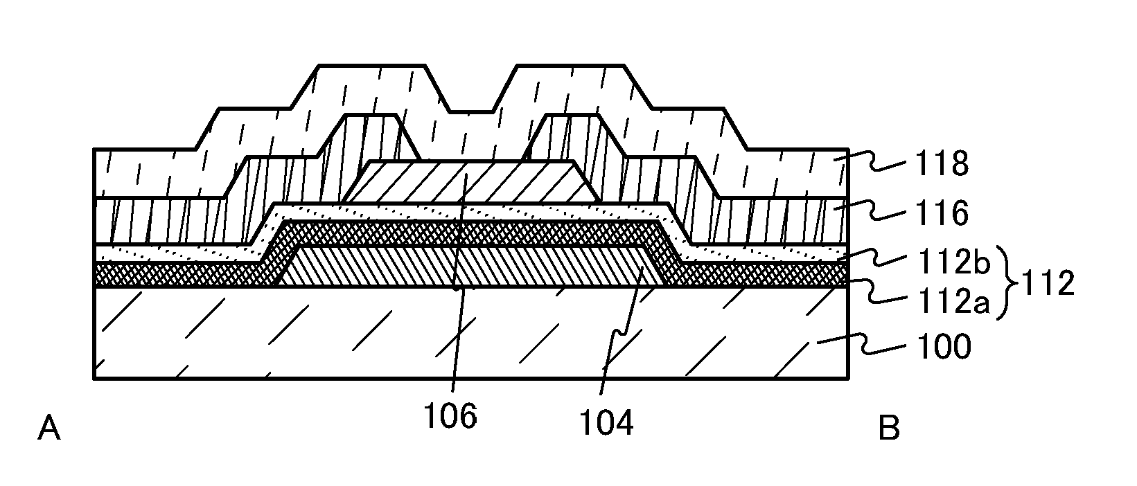
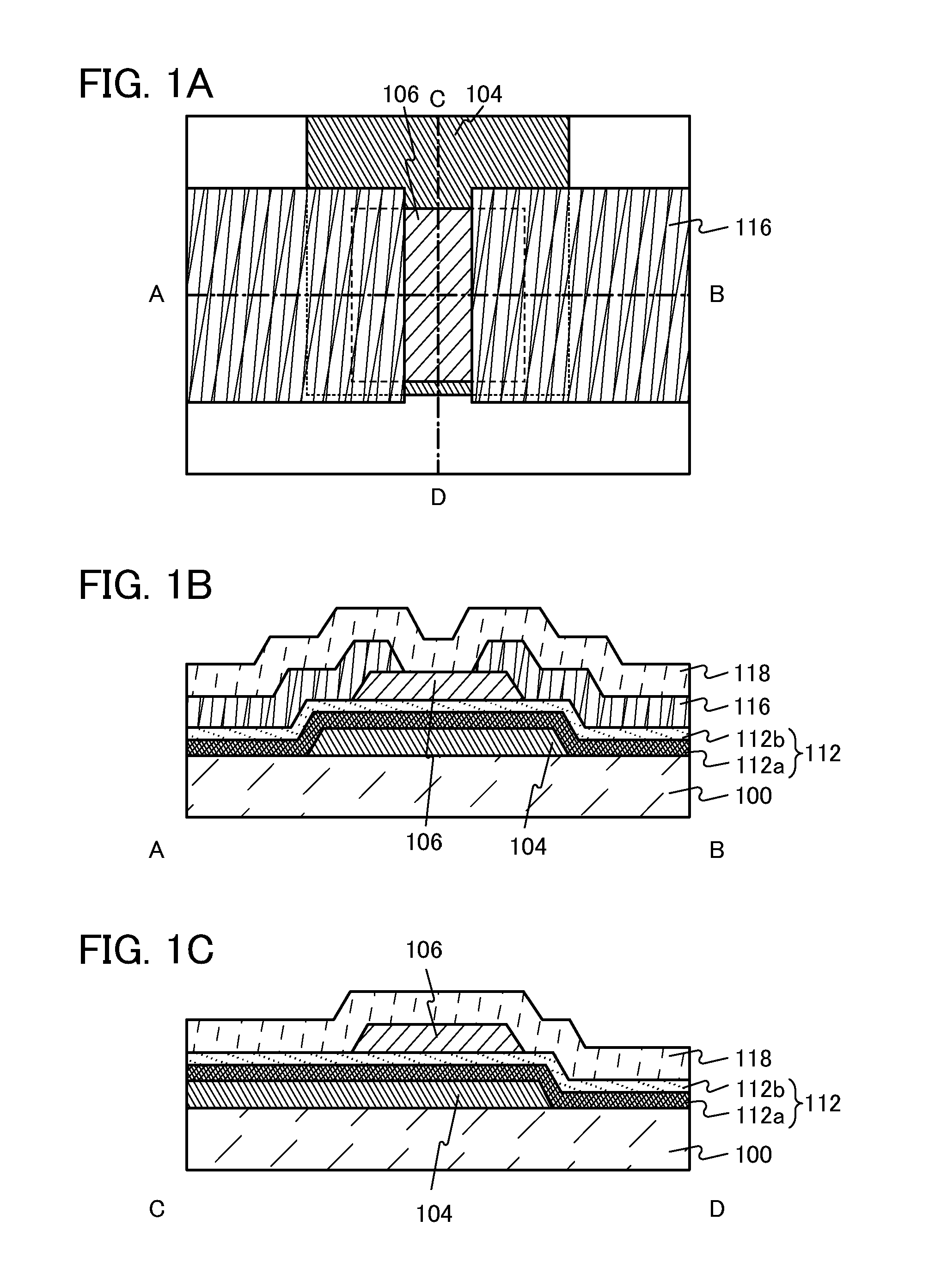
[0040]In this embodiment, an example of a transistor of one embodiment of the present invention will be described with reference to FIGS. 1A to 1C.

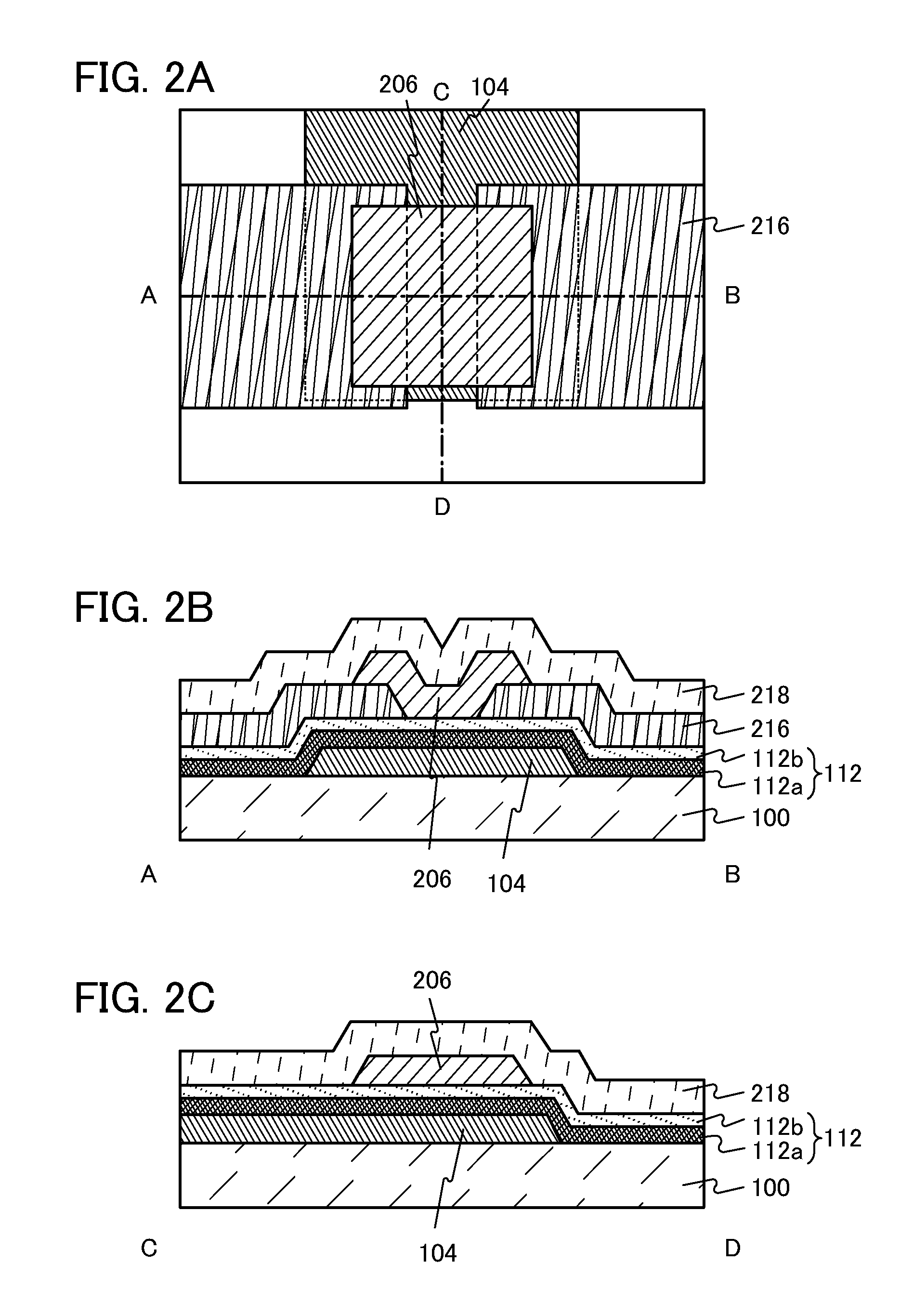
[0041]FIG. 1A is a top view of the transistor. A cross section along the dashed-dotted line A-B in FIG. 1A and a cross section along the dashed-dotted line C-D in FIG. 1A correspond to a cross section A-B in FIG. 1B and a cross section C-D in FIG. 1C, respectively.

[0042]Here, the cross section A-B in FIG. 1B will be described in detail.

[0043]The transistor includes a substrate 100, a gate electrode 104 over the substrate 100, a gate insulating film 112 which covers the gate electrode 104 and includes a first gate insulating film 112a and a second gate insulating film 112b over the first gate insulating film 112a, an oxide semiconductor film 106 which is over the gate electrode 104 with the gate insulating film 112 provided therebetween, and a pair of electrodes 116 which is over the oxide semiconductor film 106 and is partly in contact wi...

embodiment 2

[0167]In this embodiment, a liquid crystal display device manufactured using the transistor described in Embodiment 1 will be described. Note that although an example in which one embodiment of the present invention is applied to the liquid crystal display device is described in this embodiment, the present invention is not limited to this embodiment. For example, application of one embodiment of the present invention to an electroluminescence (EL) display device which is one of light-emitting devices is readily conceived by those skilled in the art.

[0168]FIG. 13 is a circuit diagram of an active matrix liquid crystal display device. The liquid crystal display device includes source lines SL_1 to SL_a, gate lines GL_1 to GL_b, and a plurality of pixels 2200. Each pixel 2200 includes a transistor 2230, a capacitor 2220, and a liquid crystal element 2210. The plurality of pixels 2200 with such a configuration forms a pixel portion of the liquid crystal display device. In the case wher...

embodiment 3

[0179]In this embodiment, an example of manufacturing a semiconductor memory device using the transistor described in Embodiment 1 will be described.

[0180]Typical examples of a volatile semiconductor memory device include a dynamic random access memory (DRAM) which stores data by selecting a transistor included in a memory element and accumulating an electric charge in a capacitor and a static random access memory (SRAM) which holds stored data using a circuit such as a flip-flop.

[0181]Typical examples of a nonvolatile semiconductor memory device include a flash memory which has a node between a gate electrode and a channel region of a transistor and stores data by holding an electric charge in the node.

[0182]The transistor described in Embodiment 1 can be applied to some of transistors included in the above-described semiconductor memory device.

[0183]First, a memory cell included in a semiconductor memory device to which the transistor described in Embodiment 1 is applied will be d...


PUM


Abstract

In the transistor including an oxide semiconductor film, a gate insulating film of the transistor including an oxide semiconductor film has a stacked-layer structure of the hydrogen capture film and the hydrogen permeable film. At this time, the hydrogen permeable film is formed on a side which is in contact with the oxide semiconductor film, and the hydrogen capture film is formed on a side which is in contact with a gate electrode. After that, hydrogen released from the oxide semiconductor film is transferred to the hydrogen capture film through the hydrogen permeable film by the heat treatment.

Description

BACKGROUND OF THE INVENTION[0001]1. Field of the Invention[0002]The present invention relates to a semiconductor device which is provided with a circuit including a semiconductor element such as a transistor. For example, the present invention relates to a power device which is mounted on a power supply circuit, a semiconductor integrated circuit including a memory, a thyristor, a converter, an image sensor, or the like, an electro-optical device typified by a liquid crystal display device, a light-emitting display device including a light-emitting element, and the like; and an electronic device on which any of the above circuit and devices are mounted as a component.[0003]In this specification, a semiconductor device generally refers to a device which can function by utilizing semiconductor characteristics; an electro-optical device, a light-emitting display device, a semiconductor circuit, and an electronic device are all included in the category of the semiconductor device.[0004]...

Claims


Application Information

Patent Timeline
Patent Type & Authority Applications(United States)
IPC IPC(8): H01L29/786H01L21/44
CPCH01L29/7869
Inventor IMOTO, YUKIMARUYAMA, TETSUNORIENDO, YUTA
Owner SEMICON ENERGY LAB CO LTD
Why Eureka
Try Eureka