NEMS comprising alsi alloy based transduction means

a transducer and alsi alloy technology, applied in the field of nems, can solve the problems of metal contamination, inconvenient measurement, and disadvantageous use of semi-conducting gauges in this application, and achieve the effect of reducing the number of metals in the sample, and improving the accuracy of measuremen

Active Publication Date: 2012-11-01
COMMISSARIAT A LENERGIE ATOMIQUE ET AUX ENERGIES ALTERNATIVES +1
View PDF4 Cites 16 Cited by
  • Summary
  • Abstract
  • Description
  • Claims
  • Application Information

AI Technical Summary

Benefits of technology

[0025]Frequency detection consists in measuring any shift in the mechanical resonance frequency of an oscillating component when it is subjected to a given stimulus. In the case of the invention, it involves measuring a frequency shift when a very small mass settles on the surface of the sensitive component. The size of the NEMS is thus favourable to attain high sensitivities. At the same time, the mechanical frequencies attained with these nano-structures are high (100 MHz and above). It is thus advantageous that the input impedances of the sensor and the electrical circuits are close and adapted 50Ω.
[0026]To resume, contrary to the prejudices existing in those skilled in the art and specialists of MEMS sensors, the choice of a thin film of aluminium alloy, to form both the piezoresistive sensitive layer and the thermoelastic actuation layer in mass sensors on NEMS, is the most adapted. It meets in fact all of the requisite conditions: low resistivity, high difference of CTE with silicon (constituting the base material of NEMS), low mass density, deposition in thin films, uniform and controllable, easy to implement, compatibility with CMOS and other microelectronic methods (VLSI).
[0028]Furthermore, a low mass density of the material is also sought for mass sensor applications where it has been demonstrated that the resolution of the sensor is proportional to its total mass. The lighter the thermoelastic actuation layer and the sensitive layer, the finer the final resolution of the system will be.

Problems solved by technology

In considering a typical doping of 1018 cm−3 conventionally used in MEMS technology, their resistances have high unit length values, which makes the measurement very awkward (reduction of the signal by resistive bridge effect for example).
The use of semi-conducting gauges for this application is thus disadvantageous compared to metal layers.
Nevertheless, the use of the latter such as gold can pose several production problems, such as the steps of etching or the non compatibility of these metals with CMOS procedures due to their highly contaminating character.
These metals are generally contaminants when they are etched.

Method used


Image

  • NEMS comprising alsi alloy based transduction means
  • NEMS comprising alsi alloy based transduction means
  • NEMS comprising alsi alloy based transduction means

Examples


Embodiment Construction

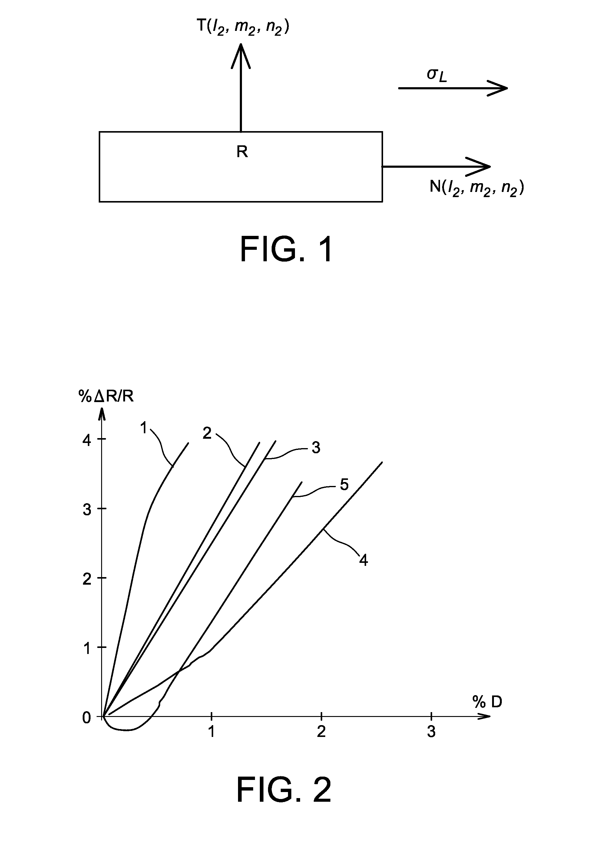
[0023]Like any metal, the gauge factor of an aluminium alloy based material is low and its resistivity is very low. In other words, that signifies that the signal applied to a sensitive component based on aluminium alloy must be very weak to avoid any fusion of the component by fusible effect. Furthermore, the transduction is not very efficient due to its low gauge factor. Since the displacements and the strains in the movable mechanical components of the microsystems are high, all of these arguments incite those skilled in the art to rule out this type of layer to form the sensitive layer.

[0024]For low deformation NEMS applications (compared to its smallest dimension) that cannot in essence accept high powers (thus high voltages), these arguments become prejudices. The sensitivity of a NEMS (particularly its capacity to be sensitive to a mass settling on its surface or to an acceleration) is no longer the major problem (in particular for frequency detection sensors). Consequently, ...


PUM

PropertyMeasurementUnit
thicknessaaaaaaaaaa
thicknessaaaaaaaaaa
thicknessaaaaaaaaaa

Abstract

The invention relates to a nano electro- mechanical system (NEMS) formed on a substrate (21) and comprising at least one fixed part associated with the substrate and at least one movable part (23) in relation to the substrate, said system comprising transduction means (24) capable of exciting the movable part to confer on it a movement and / or to detect a movement of movable part, the transduction means comprising at least one electrically conductive material. The electrically conductive material is made of an AlSi alloy based deposition, said deposition being supported at least in part by the movable part of the system.

Description

TECHNICAL FIELD[0001]The invention relates to devices known as NEMS (for “Nano Electro-Mechanical Systems”) comprising at least one movable part associated with transduction means (of excitation and / or detection).STATE OF THE PRIOR ART[0002]The development of NEMS necessitates developing integrable actuation and detection principles, adapted to detecting slight deformations at high frequencies compared to the displacements and frequencies brought into play in micro-sensors, produced by MEMS (for “Micro Electro-Mechanical Systems”) technologies. The principles available must make it possible to design simple patterns and production methods. The techniques implemented must remain compatible with the tools and methods of microelectronics so that their very large scale integration, via clean rooms or microelectronic foundries, is accessible. In this spirit, the pertinence of the principles of thermoelastic actuation and piezoresistive detection has been demonstrated. Reference may be ma...

Claims


Application Information

Patent Timeline
Patent Type & Authority Applications(United States)
IPC IPC(8): G01L1/18B81B3/00
CPCG01N2291/0427G01N2291/014G01P15/123G01P15/097B81B2203/0118G01N29/022B81B2203/058B81B3/0021
Inventor ANDREUCCI, PHILIPPEDURAFFOURG, LAURENTMARCOUX, CARINEBRIANCEAU, PIERREHENTZ, SEBASTIENMINORET, STEPHANEMYERS, EDWARDROUKES, MICHAEL
Owner COMMISSARIAT A LENERGIE ATOMIQUE ET AUX ENERGIES ALTERNATIVES
Why Eureka
Try Eureka