

Gain cell semiconductor memory device and driving method thereof
a semiconductor memory and gain cell technology, applied in semiconductor devices, digital storage, instruments, etc., can solve the problem of becoming more and more difficult to keep the necessary capacitan
- Summary
- Abstract
- Description
- Claims
- Application Information
AI Technical Summary
Benefits of technology
Problems solved by technology
Method used
Image

Examples
embodiment 1
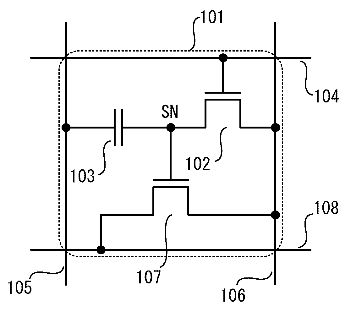
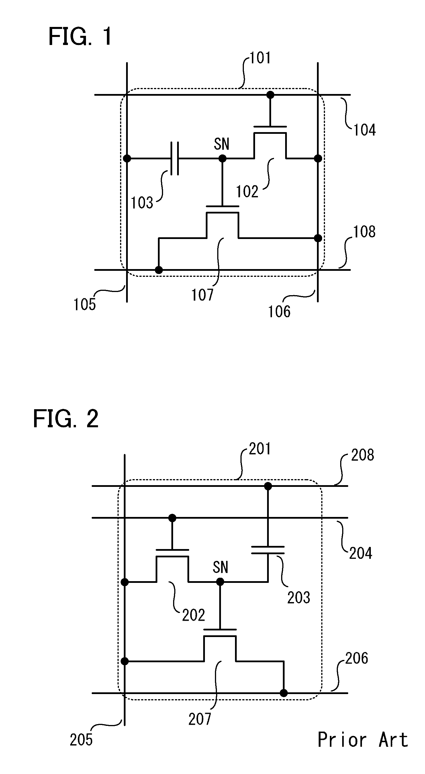
[0039]FIG. 1 is a circuit diagram of a memory cell of a semiconductor memory device of this embodiment. A memory cell 101 includes one write transistor 102, one read transistor 107, and one capacitor 103. A gate of the write transistor 102 is connected to a write word line 104, and a source of the write transistor 102 is connected to a source line 106.
[0040]A first electrode of the capacitor 103 is connected to a drain of the write transistor 102. This node is referred to as a storage node SN. A second electrode of the capacitor 103 is connected to a write bit line 105.
[0041]A gate of the read transistor 107 is connected to the storage node SN, a drain of the read transistor 107 is connected to a read line 108, and a source of the read transistor 107 is connected to the source line 106. Note that the read line 108 is preferably arranged to be orthogonal to (intersecting with) the source line 106.
[0042]In FIG. 1, the source line 106 is provided in parallel to the write bit line 105; ...
embodiment 2
[0066]In a memory cell of a semiconductor memory device of this embodiment, the conductivity type of the read transistor 107 in FIG. 1 is different from the conductivity type of the write transistor 102. For example, when the write transistor 102 is an n-channel transistor, the read transistor 107 is a p-channel transistor.
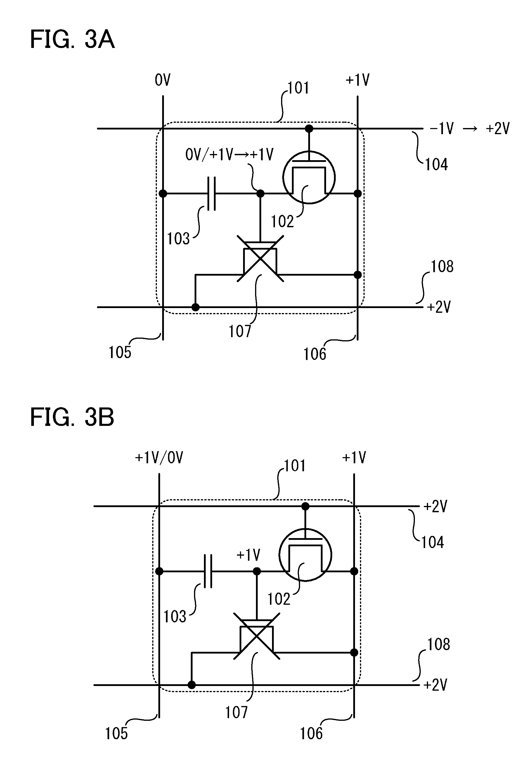
[0067]Examples of methods for writing data to and reading data from the semiconductor memory device of this embodiment will be briefly described with reference to FIGS. 6A to 6C and FIGS. 7A to 7C. Two memory cells 101_1 and 101_2 are illustrated in each of FIGS. 6A to 6C and FIGS. 7A to 7C. Data is input to the memory cell 101_1 through a write bit line 105_1, and data is input to the memory cell 101_2 through a write bit line 105_2. In an example described below, after data is written to the memory cell 101_1, the data is read from the memory cell 101_1 while data in the memory cell 101_2 is retained and is not read.
[0068]Specific values are given below as poten...
embodiment 3
[0095]In this embodiment, steps of manufacturing the semiconductor memory device described in the above embodiment will be briefly described with reference to FIGS. 8A and 8B, FIGS. 9A and 9B, and FIGS. 10A to 10C. FIGS. 8A and 8B and FIGS. 9A and 9B are schematic cross-sectional views, and FIGS. 10A to 10C are schematic views of some of components seen from the above. Note that FIGS. 8A and 8B and FIGS. 9A and 9B are the cross-sectional views taken along dashed-dotted lines A-B in FIGS. 10A to 10C. Note that a known semiconductor manufacturing technique or Patent Document 2 can be referred to for the detail of some of the steps.
8A>
[0096]An element separation region 111 and the like are formed at a substrate 110 formed using a semiconductor such as silicon, gallium arsenide, gallium phosphide, or germanium. Further, read gates 112_1 and 112_2 which are gates of read transistors are formed, and impurity regions 113_1 to 113_4 are formed.
[0097]The impurity regions 113_1 and 113_3 serv...
PUM
 Abstract
Description
Claims
Application Information