
Semiconductor element mounting member, method of producing the same, and semiconductor device

Inactive Publication Date: 2012-11-22
ALLIED MATERIAL
View PDF2 Cites 0 Cited by
  • Summary
  • Abstract
  • Description
  • Claims
  • Application Information

AI Technical Summary

Benefits of technology

[0031]It is an object of the present invention to provide a semiconductor element mounting member that has a high thermal conductivity meeting the fact of being formed by use of diamond particles and that is capable of arbitrarily enlarging its size without undergoing the restriction of, for example, manufacturing facilities.
[0032]It is another object of the present invention to provide a method of producing the semiconductor element mounting member efficiently at a low cost without using large-scale manufacturing facilities.
[0033]It is still another object of the present invention to provide a semiconductor device that is capable of promptly removing heat generated during the operation of a semiconductor element by using the semiconductor element mounting member and that is capable of reliably preventing the semiconductor element from making a malfunction caused by heat, or from lowering its operation efficiency and its lifetime, or from being damaged.

Problems solved by technology

However, in this production method, special manufacturing facilities that can create the high-temperature / extra-high-pressure condition are needed, and therefore the restriction of the manufacturing facilities imposes inevitable limitations on the size of a producible semiconductor-element mounting member.
Additionally, the heat treatment and the pressure treatment are performed according to so-called batch processing, and require much time for one-time processing, and consume enormous energy, and therefore the productivity of the semiconductor element mounting member is remarkably low.
Additionally, large-scale manufacturing facilities are needed in comparison with the size of a precursor that can be formed, and, as a result, disadvantageously, production costs of the semiconductor element mounting member become high.
However, a problem resides in the fact that, although the semiconductor element mounting member that is produced through the infiltration step of each of Patent Documents 2 and 3 is formed by use of diamond particles, the semiconductor element mounting member cannot obtain a high thermal conductivity resulting from the use of diamond particles.
The cause is that the infiltration auxiliary layer formed on substantially the whole of the surface of diamond particles hinders the diamond particles from coming into direct contact with each other, and hence brings about a decrease in thermal conductivity between the diamond particles.
Another problem resides in the fact that the number of process steps is increased, and the productivity of the semiconductor element mounting member is lowered in accordance with the necessity of the process of forming the infiltration auxiliary layer on the diamond-particle surface.

Method used


Image

  • Semiconductor element mounting member, method of producing the same, and semiconductor device
  • Semiconductor element mounting member, method of producing the same, and semiconductor device

Examples


examples 2 to 7

[0263]A diamond-Cu complex serving as a precursor of the semiconductor element mounting member was obtained in the same way as in Example 1 except for the fact that the volume ratio between the diamond particles and the Cr powder was adjusted so that the content percentage of Cr was 0.11 volume % (Example 2), 1.25 volume % (Example 3), 5.5 volume % (Example 4), 7 volume % (Example 5), 16 volume % (Example 6), and 21 volume % (Example 7) of the total amount of Cr and the diamond particles.

[0264]The mixing ratio of the ammonium chloride powder was adjusted so that the atomic ratio M / X maintained 1 / 2.7.

examples 8 and 9

[0265]A diamond-Cu complex serving as a precursor of the semiconductor element mounting member was obtained in the same way as in Example 1 except for the fact that the mixing ratio of the ammonium chloride powder was adjusted so that the atomic ratio M / X was 1 / 1.7 (Example 8) and 1 / 2.1 (Example 9).

[0266]The volume ratio between the diamond particles and the Cr powder was set to be 95:5. The content percentage of Cr was 5 volume % of the total amount of Cr and the diamond particles.

[0267]In Example 8, unevenness occurred in the infiltration auxiliary layer, and therefore many bubbles were observed after the infiltration of Cu.

examples 10 to 14

[0268]A diamond-Cu complex serving as a precursor of the semiconductor element mounting member was obtained in the same way as in Example 1 except for the fact that diamond particles having a mean particle diameter of 0.6 μm (Example 10), 3 μm (Example 11), 11 μm (Example 12), 48 μm (Example 13), and 193 μm (Example 14) were used as the diamond particles.

[0269]The volume ratio between the diamond particles and the Cr powder was set to be 95:5. The content percentage of Cr was 5 volume % of the total amount of Cr and the diamond particles.

[0270]Additionally, the mixing ratio between the Cr powder and the ammonium-chloride powder was 1 / 2.7 that was expressed as the atomic ratio M / X.

[0271]In Example 14, a major defect that was caused by the drop-off of diamond particles during grinding was observed.


PUM

PropertyMeasurementUnit
Temperatureaaaaaaaaaa
Thicknessaaaaaaaaaa
Diameteraaaaaaaaaa

Abstract

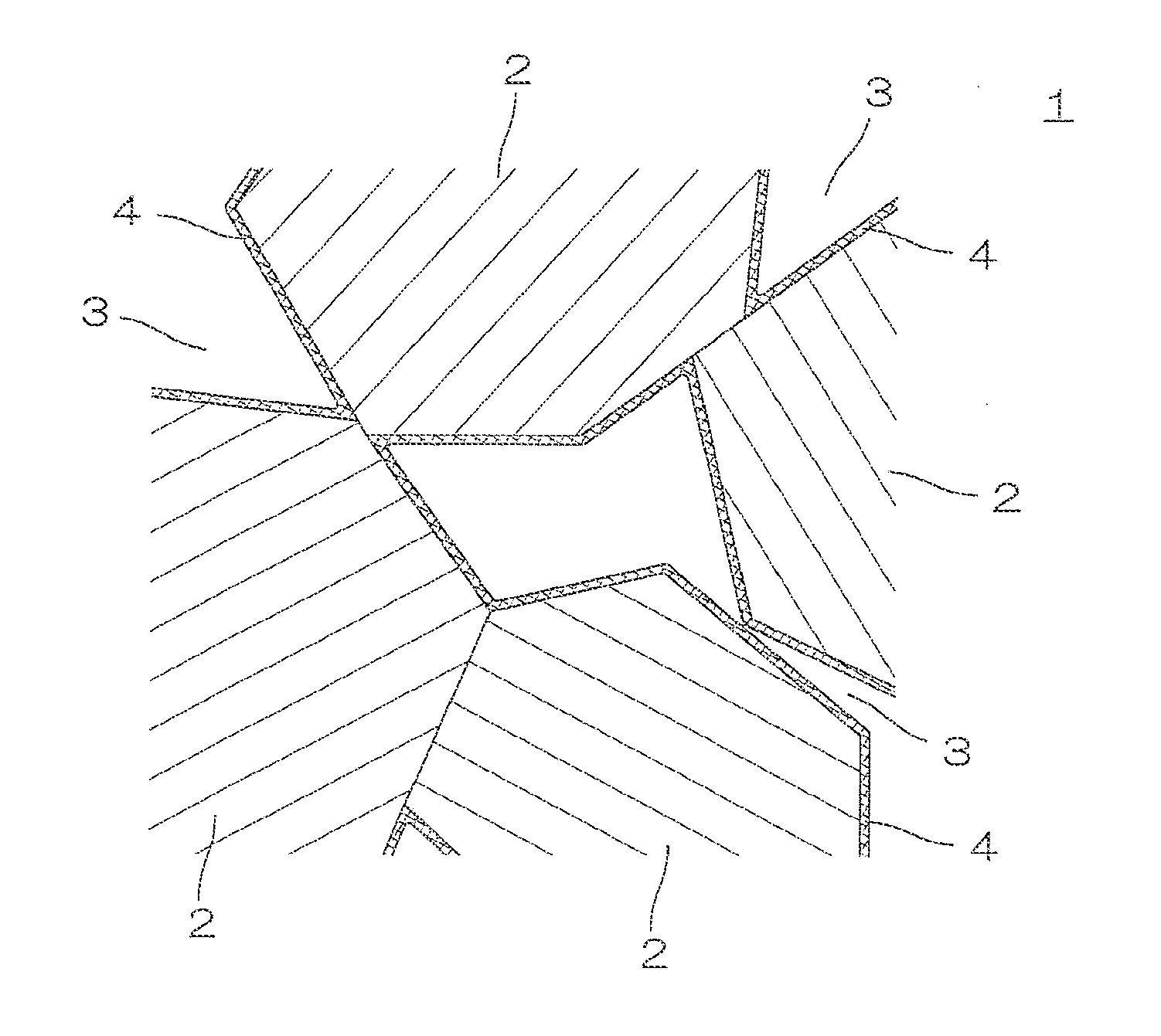
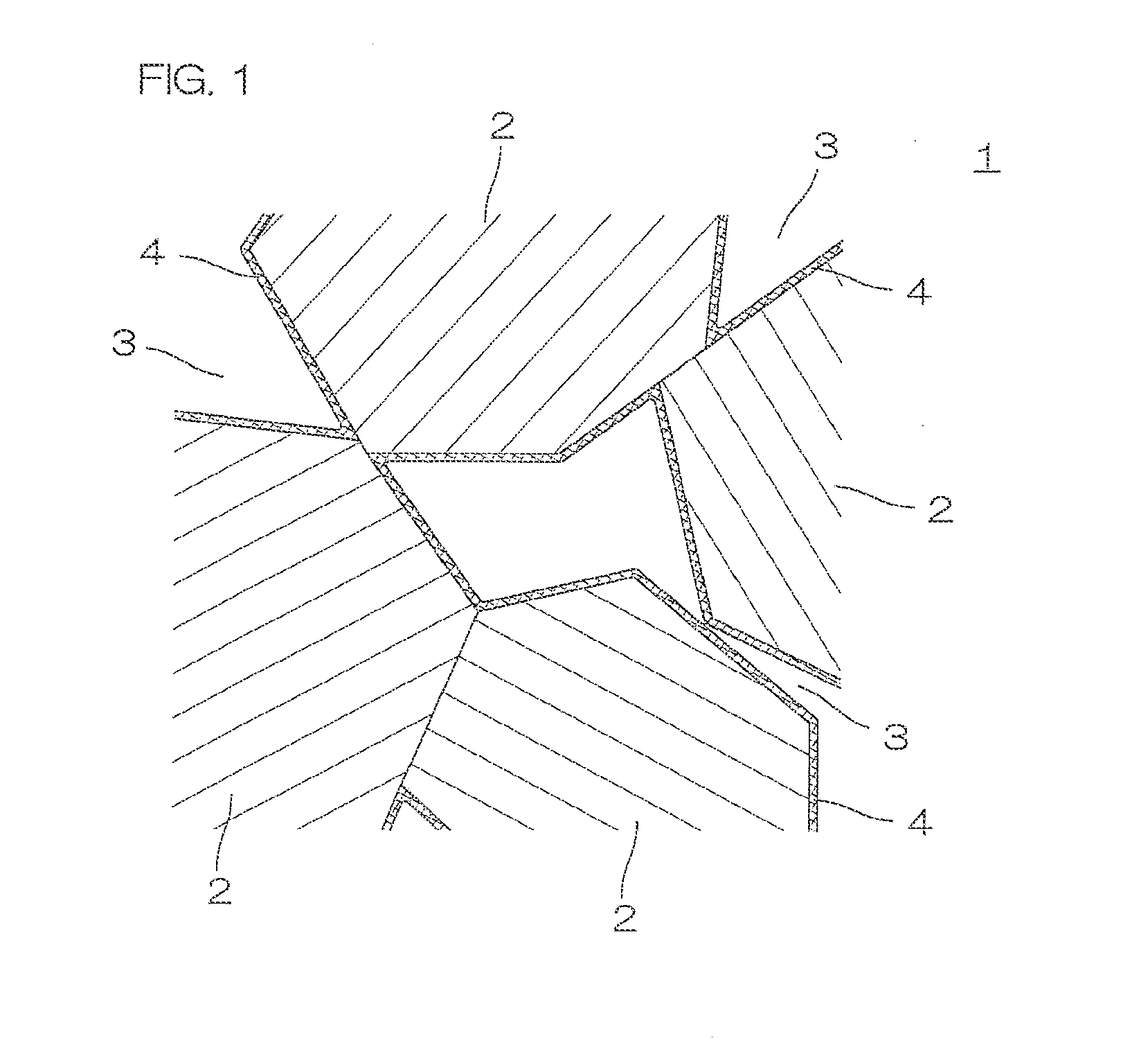
A semiconductor element mounting member is arranged to infiltrate a matrix metal into a porous body that is formed by sintering diamond particles being in direct contact with each other and that has an infiltration auxiliary layer selectively formed only on the exposed surface of each diamond particle. A production method includes a step at which a mixture of diamond particles, a powder of a chemical element out of which the infiltration auxiliary layer is made, and an ammonium chloride powder is compressed and molded, is then heated to 900° C. or more, and is formed into the porous body. A semiconductor device has a semiconductor element mounted on an element mounting surface of the semiconductor element mounting member with a connecting layer therebetween.

Description

CROSS-REFERENCE TO RELATED APPLICATIONS[0001]The present application is a continuation of pending International patent application PCT / JP2011 / 051925 filed on Jan. 31, 2011 which designates the United States and claims priority from Japanese patent application 2010-025480 filed on Feb. 8, 2010, the content of which is incorporated herein by reference.FIELD OF THE INVENTION[0002]The present invention relates to a semiconductor element mounting member that consists of a diamond-metal complex including many diamond particles and a matrix metal and that has an element mounting surface on which a semiconductor element is mounted, relates to a method of producing the semiconductor element mounting member, and relates to a semiconductor device that uses the semiconductor element mounting member.BACKGROUND OF THE INVENTION[0003]A semiconductor-element mounting member (e.g., a submount, a heat spreader, a heat sink, or a housing) which has an element mounting surface on which a semiconductor ...

Claims


Application Information

Patent Timeline
IPC IPC(8): H01L23/498B22F3/12B29C67/04H05K7/20
CPCH01L23/3732H01L2924/0002H01L2924/00
Inventor TAKASHIMA, KOUICHIAOI, YOSHIFUMIKAMIJO, EIJI
Owner ALLIED MATERIAL
Learn More