Semiconductor device

a technology of semiconductors and devices, applied in the direction of instruments, computations using denominational number representations, pulse techniques, etc., can solve the problems of difficult to achieve high-speed operation, power consumption reduction, and loss of stored data, and achieve the effect of high speed

Inactive Publication Date: 2012-11-22
SEMICON ENERGY LAB CO LTD
View PDF13 Cites 54 Cited by
  • Summary
  • Abstract
  • Description
  • Claims
  • Application Information

AI Technical Summary

Benefits of technology

[0011]When flash memory, which is nonvolatile, is used as the storage circuit, data can be maintained even after supply of power supply voltage is stopped. However, it is difficult to achieve high-speed operation and reduce power consumption because the drive voltage of flash memory is high.
[0012]In view of the above, an object of one embodiment of the present invention is to provide a semiconductor device that can maintain the connection relation between logic circuit units or the circuit configuration of each of the logic circuit units for a long time even after supply of power supply voltage is stopped.
[0013]Another object of one embodiment of the present invention is to provide a semiconductor device in which the connection relation between logic circuit units or the circuit configuration of each of the logic circuit units can be changed at high speed.
[0021]According to one embodiment of the present invention, it is possible to provide a semiconductor device that can maintain data on the connection relation between logic circuit units or data on the circuit configuration of each of the logic circuit units for a long time even after supply of power supply voltage is stopped.
[0022]Moreover, according to one embodiment of the present invention, it is possible to provide a semiconductor device in which the connection relation between logic circuit units or the circuit configuration of each of the logic circuit units can be changed at high speed or with low power consumption.

Problems solved by technology

However, since SRAM and DRAM are volatile, stored data is lost when supply of power supply voltage is stopped.
However, it is difficult to achieve high-speed operation and reduce power consumption because the drive voltage of flash memory is high.

Method used


Image

  • Semiconductor device
  • Semiconductor device
  • Semiconductor device

Examples


embodiment 1

[0059]In this embodiment, an example of a semiconductor device will be described.

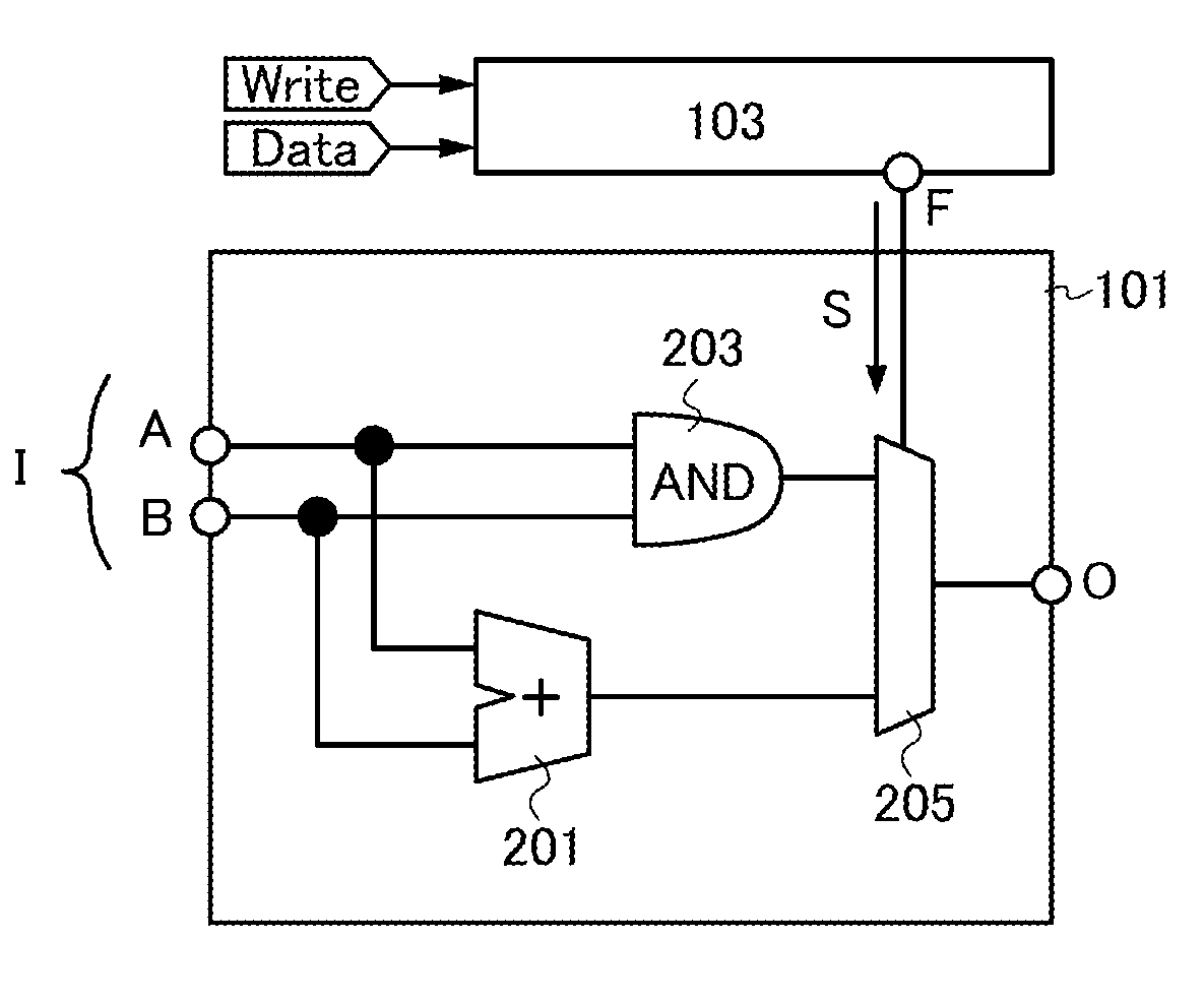
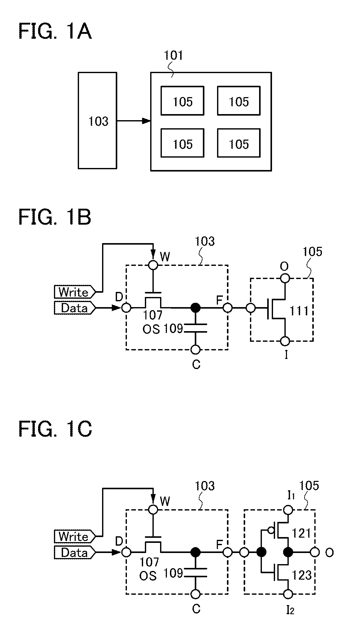
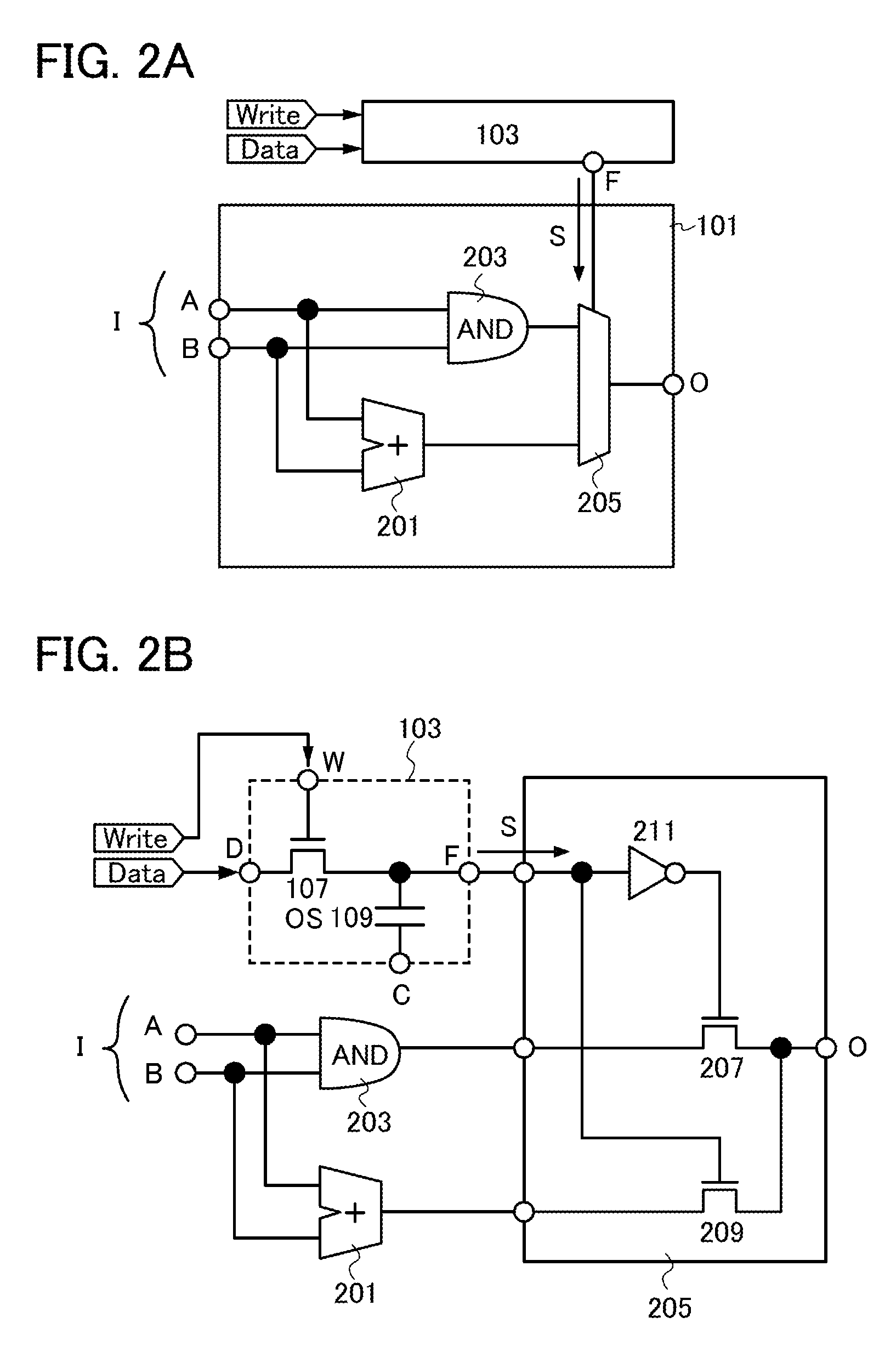
[0060]FIG. 1A is an example of a block diagram of a semiconductor device.

[0061]The semiconductor device in FIG. 1A includes a logic circuit unit 101 and a storage circuit 103. The logic circuit unit 101 includes a plurality of logic circuits 105. In the semiconductor device, at least one of the plurality of logic circuits 105 is selected in accordance with data (also referred to as signal) stored in the storage circuit 103, and the circuit configuration of the logic circuit unit 101 is determined

[0062]An example of the logic circuit unit 101 is an ALU. Examples of the plurality of logic circuits 105 are operation circuits such as an adder, a subtractor, a multiplier, an AND circuit, an OR circuit, a NOT circuit, an XOR circuit, and a shift circuit; and selector circuits such as a multiplexer. Alternatively, the logic circuit 105 may be one element such as one transistor. It can be said that the logic ci...

embodiment 2

[0101]In this embodiment, an example of a semiconductor device different from that in Embodiment 1 will be described.

[0102]FIGS. 4A and 4B each illustrate a variation example of FIG. 1B.

[0103]First, the example in FIG. 4A is described. The storage circuit 103 is the same as that in FIG. 1B and the like.

[0104]The logic circuit 105 in FIG. 4A includes the transistor 111, a transistor 401, and an inverter 403. The transistor 111 and the transistor 401 are electrically connected in parallel to each other between the terminal I and the terminal O. That is, one of the source and the drain of the transistor 111 and one of a source and a drain of the transistor 401 are electrically connected to the terminal I, and the other of the source and the drain of the transistor 111 and the other of the source and the drain of the transistor 401 are electrically connected to the terminal O.

[0105]The transistors 111 and 401 have different polarities; one of the transistors 111 and 401 is an n-channel ...

embodiment 3

[0110]In this embodiment, an example of a semiconductor device different from those in Embodiments 1 and 2 will be described.

[0111]A semiconductor device in FIG. 5A includes a plurality of logic circuit units 101 and a connector unit 501. The logic circuit unit 101 is the same as those in FIGS. 1A to 1C, FIGS. 2A and 2B, and FIG. 3 and can be an ALU or the like.

[0112]The connector unit 501 has a function of controlling electrical continuity of wirings 503 with which the plurality of logic circuit units 101 are electrically connected to each other. FIG. 5B illustrates the connector unit 501 in detail.

[0113]The circuit configuration and driving method of the connector unit 501 in FIG. 5B are the same as those in FIG. 1B; the on / off state of the transistor 111 is controlled in accordance with the data Data of the storage circuit 103. That is, electric conduction between the terminal I and the terminal O is controlled. The terminal I and the terminal O are electrically connected to diff...


PUM


Abstract

An object is to provide a semiconductor device that can maintain the connection relation between logic circuit units or the circuit configuration of each of the logic circuit units even after supply of power supply voltage is stopped. Another object is to provide a semiconductor device in which the connection relation between logic circuit units or the circuit configuration of each of the logic circuit units can be changed at high speed. In a reconfigurable circuit, an oxide semiconductor is used for a semiconductor element that stores data on the circuit configuration, connection relation, or the like. Specifically, the oxide semiconductor is used for a channel formation region of the semiconductor element.

Description

BACKGROUND OF THE INVENTION[0001]1. Field of the Invention[0002]The technical field relates to a semiconductor device, a method for driving a semiconductor device, and a method for manufacturing a semiconductor device. The semiconductor device is particularly a semiconductor integrated circuit including a semiconductor element such as a transistor.[0003]2. Description of the Related Art[0004]A programmable logic device (PLD) is one of semiconductor integrated circuits. A PLD is an integrated circuit having an internal configuration that can be determined and altered (is reconfigurable) after manufacture (see Patent Document 1).[0005]A PLD has the following advantages, for example, over a conventional application specific integrated circuit (ASIC): the development period can be shortened and a PLD enables flexible response to a change in design specification. Accordingly, PLDs are used in various kinds of devices.[0006]A PLD includes, for example, a plurality of logic circuit units a...

Claims


Application Information

Patent Timeline
Patent Type & Authority Applications(United States)
IPC IPC(8): H03K19/173
CPCH03K19/1737H03K19/17776H03K19/17772H03K19/17728H03K19/17758H01L27/1214H01L27/1225G11C11/4096
Inventor FUJITA, MASASHISHIONOIRI, YUTAKAKATO, KIYOSHIKOBAYASHI, HIDETOMO
Owner SEMICON ENERGY LAB CO LTD
Why Eureka
Try Eureka