Method for driving semiconductor device

Inactive Publication Date: 2012-11-22
SEMICON ENERGY LAB CO LTD
View PDF0 Cites 38 Cited by
  • Summary
  • Abstract
  • Description
  • Claims
  • Application Information

AI Technical Summary

Benefits of technology

[0026]Since the off-state current of a transistor including an oxide semiconductor used in an embodiment of the present invention is extremely small, stored data can be held for an extremely long time by using the transistor. In other words, power consumption can be reduced because refresh operation becomes unnecessary or the frequency of refresh operation can be extremely low. Moreover, stored data can be held for a long period even when power is not supplied (note that a potential is preferably fixed).
[0027]Further, a semiconductor device according to an embodiment of the present invention does not need high voltage for writing of data and there is no problem of deterioration of elements. For example, unlike the above-described flash memory, it is not necessary to inject and extract electrons into and from a floating gate, and thus a problem such as deterioration of a gate insulating layer does not arise at all. That is, the semiconductor device according to an embodiment of the disclosed invention does not have a limitation on the number of times of rewriting of data, which is a problem of a conventional nonvolatile memory, and the reliability thereof is drastically improved. Furthermore, since data is written by turning on or off the transistor, high-speed writing can be easily realized.

Problems solved by technology

Moreover, since leakage current (off-state current) flows between a source and a drain of a transistor included in a storage element when the transistor is in an off state for example, electric charge flows into or out even if the transistor is not selected, which makes a data holding period short.
For that reason, another writing operation (refresh operation) is necessary at predetermined intervals, and it is difficult to sufficiently reduce power consumption.
Furthermore, since stored data is lost when power is not supplied, an additional storage device using a magnetic material or an optical material is needed in order to hold the data for a long time.
However, cost per storage capacity is increased because a circuit such

Method used


Image

  • Method for driving semiconductor device
  • Method for driving semiconductor device
  • Method for driving semiconductor device

Examples


Example

Embodiment 1

[0064]In this embodiment, circuit configurations and operations of a semiconductor device according to an embodiment of the disclosed invention will be described with reference to FIGS. 1A-1, 1A-2, and 1B, FIGS. 2A and 2B, FIG. 3, FIG. 4, FIG. 5, FIG. 6, FIG. 7, FIG. 8, FIG. 9, FIG. 10, and FIG. 11. Note that in each of the circuit diagrams, “OS” may be written beside a transistor in order to indicate that the transistor includes an oxide semiconductor. The point of an embodiment of the present invention is to provide a semiconductor device including a transistor whose off-state current is very small, and thus, a transistor including a material other than an oxide semiconductor whose off-state current is small may also be used instead of a transistor including an oxide semiconductor.

1>

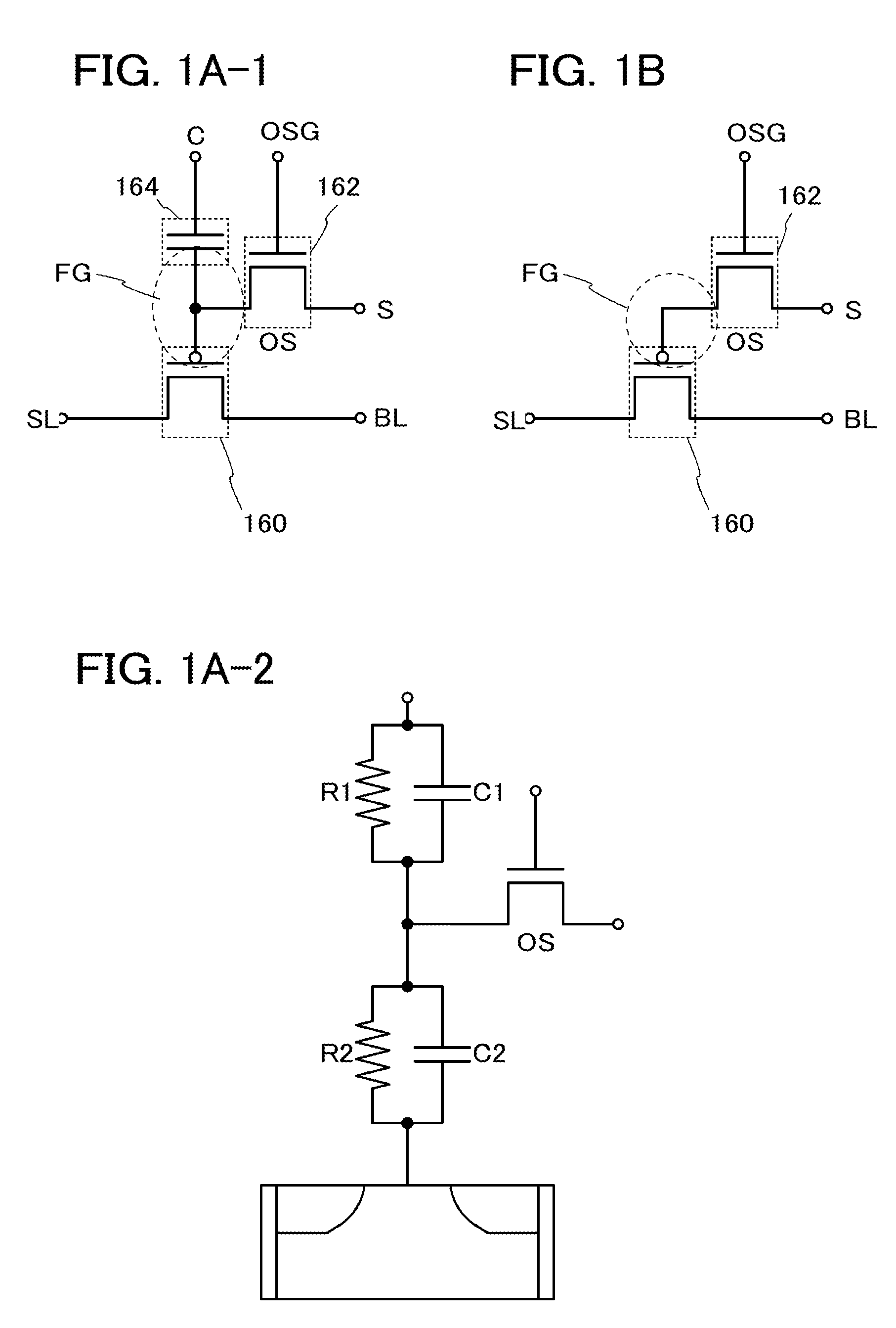
[0065]First, the most basic circuit configuration and its operation will be described with reference to FIGS. 1A-1, 1A-2, and 1B. In a semiconductor device illustrated in FIG. 1A-1, a sourc...

Example

Application Example 1

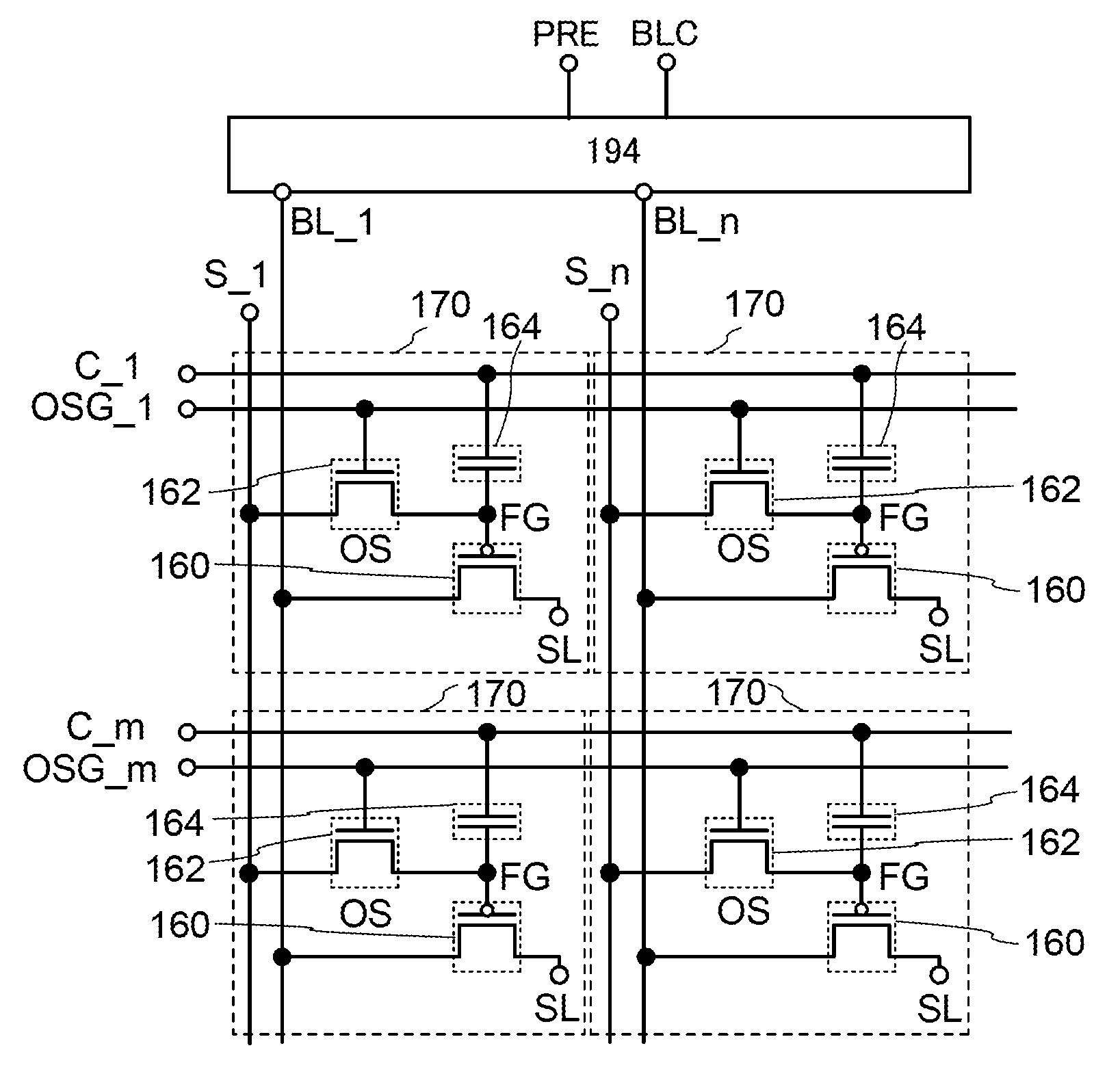
[0114]Next, a more specific circuit configuration to which the circuit illustrated in FIGS. 1A-1, 1A-2, and 1B is applied will be described with reference to FIG. 3. Note that the case where an n-channel transistor is used as a writing transistor (the transistor 162) and a p-channel transistor is used as a reading transistor (the transistor 160) will be described below as an example. Note that in the circuit diagram illustrated in FIG. 3, wirings with slashes are wirings each including a plurality of signal lines.

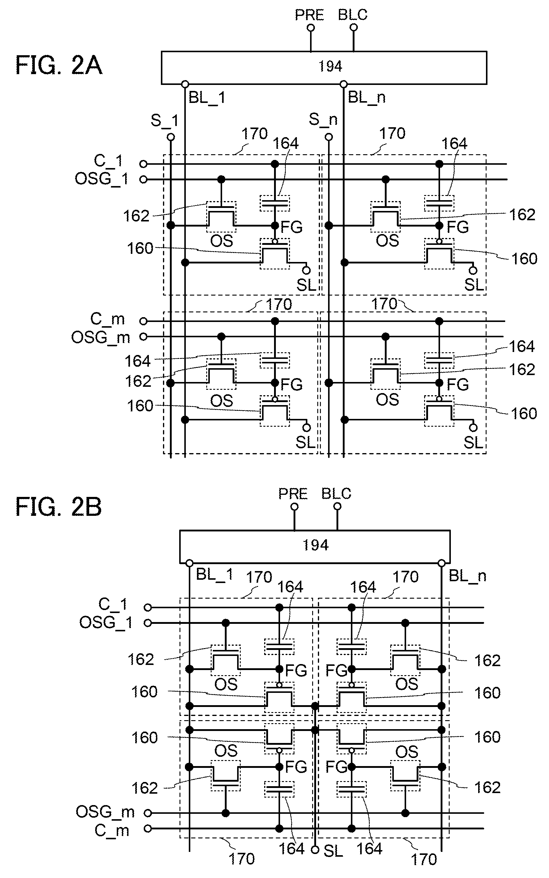
[0115]FIG. 3 is an example of a circuit diagram of a semiconductor device including (m×n) memory cells 170. The configuration of the memory cells 170 in FIG. 3 is similar to that in FIG. 1A-1.

[0116]The semiconductor device illustrated in FIG. 3 includes m (m is an integer of greater than or equal to 2) write word lines OSG, m capacitor lines C, n (n is an integer of greater than or equal to 2) bit lines BL, a source line SL, a memory cell array having t...

Example

Embodiment 2

[0153]In this embodiment, a structure and a manufacturing method of a semiconductor device according to an embodiment of the disclosed invention will be described with reference to FIGS. 12A and 12B, FIGS. 13A to 13G, FIGS. 14A to 14E, FIGS. 15A to 15D, FIGS. 16A to 16D, FIGS. 17A to 17C, FIGS. 18A to 18E, FIGS. 19A to 19C, FIGS. 20A to 20C, FIGS. 21A and 21B, FIG. 22, FIGS. 23A to 23C, FIGS. 24A to 24C, FIGS. 25A to 25C, FIGS. 26A and 26B, FIGS. 27A and 27B, FIG. 28, FIG. 29, and FIGS. 30A and 30B.

[0154]In FIGS. 12A and 12B, an example of the structure of the semiconductor device is illustrated. FIG. 12A is a cross-sectional view of the semiconductor device, and FIG. 12B is a top view of the semiconductor device. Here, FIG. 12A corresponds to a cross section taken along lines A1-A2 and B1-B2 of FIG. 12B. The semiconductor device illustrated in FIGS. 12A and 12B includes a transistor 160 including a first semiconductor material in a lower portion, and a transistor 162 in...


PUM


Abstract

A semiconductor device includes a nonvolatile memory cell including a writing transistor including an oxide semiconductor, a reading transistor including a semiconductor material different from that of the writing transistor, and a capacitor. Data is written to the memory cell by turning on the writing transistor so that a potential is supplied to a node where a source electrode of the writing transistor, one electrode of the capacitor, and a gate electrode of the reading transistor are electrically connected, and then turning off the writing transistor so that a predetermined potential is held in the node. Data is read out from the memory cell by supplying a precharge potential to a bit line, stopping the supply of the potential to the bit line, and determining whether the potential of the bit line is kept at the precharge potential or decreased.

Description

BACKGROUND OF THE INVENTION[0001]1. Field of the Invention[0002]The disclosed invention relates to a semiconductor device including a semiconductor element and a method for driving the semiconductor device.[0003]2. Description of the Related Art[0004]Storage devices using semiconductor elements are broadly classified into two categories: a volatile device that loses stored data when power is not supplied, and a nonvolatile device that holds stored data even when power is not supplied.[0005]A typical example of a volatile storage device is a dynamic random access memory (DRAM). A DRAM stores data in such a manner that a transistor included in a storage element is selected and electric charge is accumulated in a capacitor.[0006]When data is read from a DRAM, electric charge in a capacitor is lost on the above-described principle; thus, another writing operation is necessary every time data is read. Moreover, since leakage current (off-state current) flows between a source and a drain ...

Claims


Application Information

Patent Timeline
IPC IPC(8): G11C11/24
CPCG11C11/404G11C16/0433H01L27/1255H01L27/1225H01L27/1156H10B41/70G11C7/10G11C7/12H01L27/1214
Inventor MATSUZAKI, TAKANORIINOUE, HIROKINAGATSUKA, SHUHEI
Owner SEMICON ENERGY LAB CO LTD
Why Eureka
Try Eureka