Resistive random access memory with electric-field strengthened layer and manufacturing method thereof
- Summary
- Abstract
- Description
- Claims
- Application Information
AI Technical Summary
Benefits of technology
Problems solved by technology
Method used
Image

Examples
Embodiment Construction
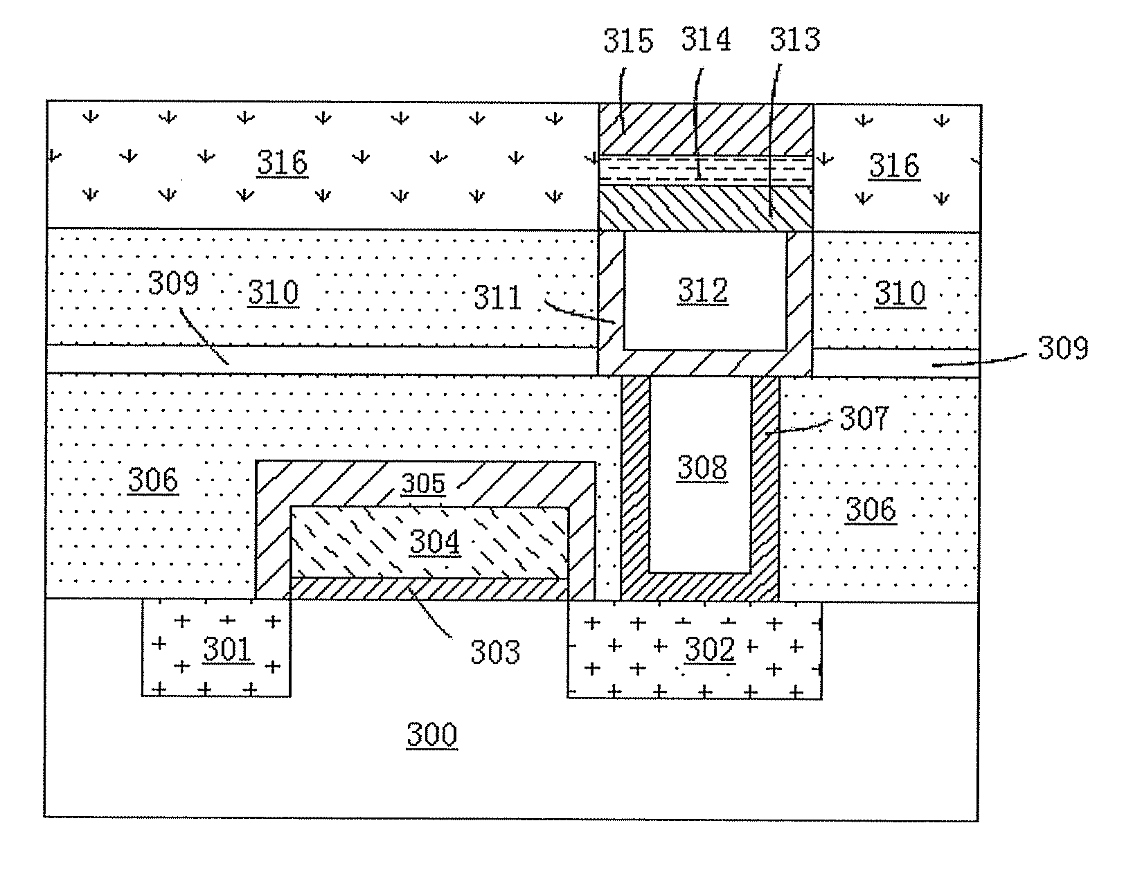
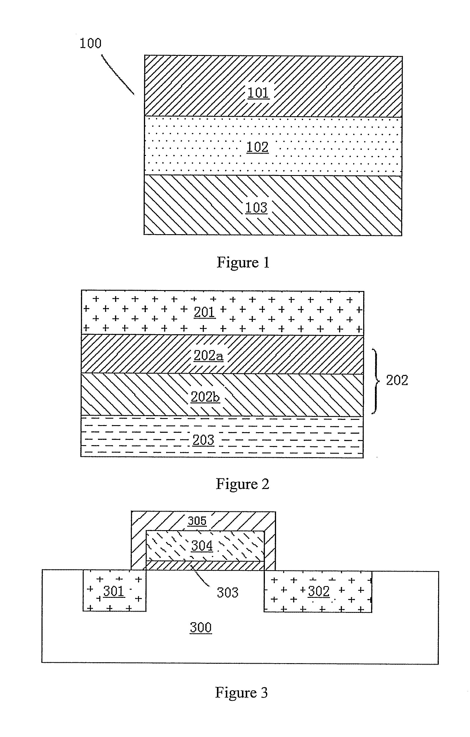
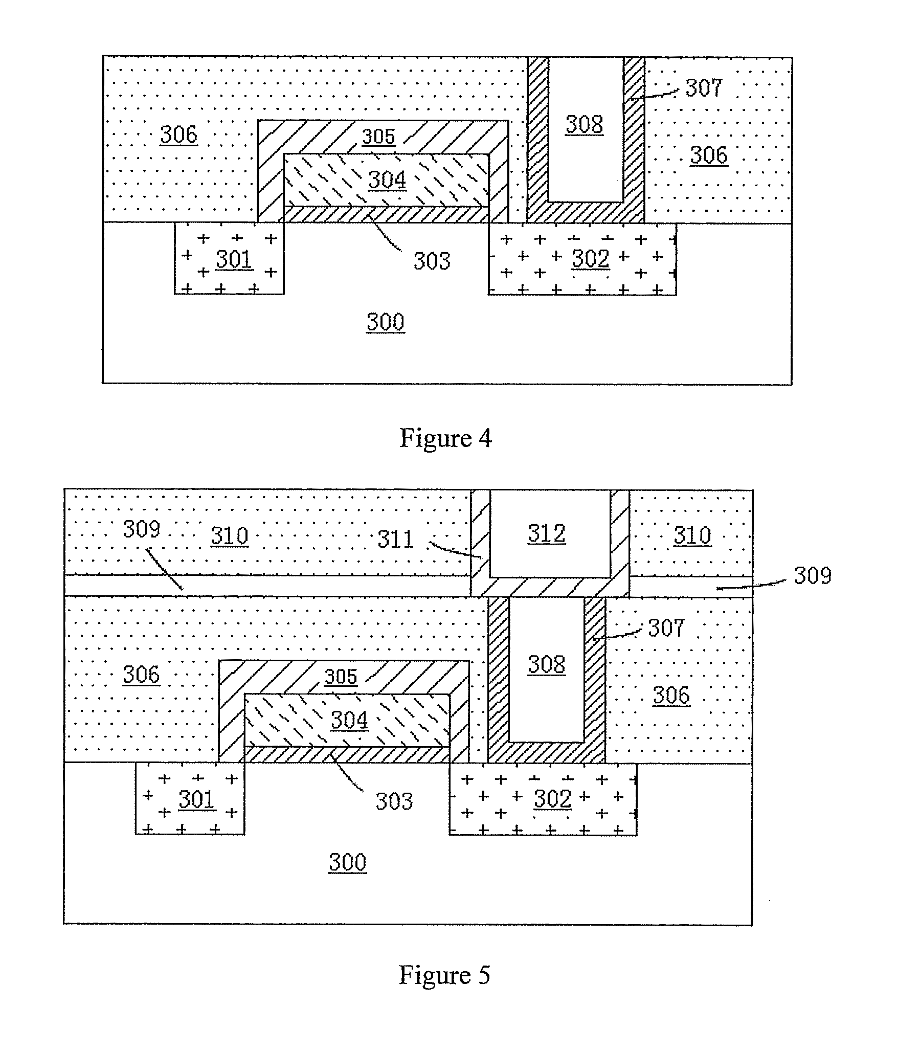
[0024]The invention is further described in detail by combining the attached drawings and the embodiments. In the figure, to facilitate description, the layer thickness and region thickness are amplified, but the sizes do not represent the actual dimensions. The figures fail to reflect the actual dimensions of the device accurately, but show the mutual positions of the regions and the structures, especially the vertical and horizontal neighborhood of the structures.
[0025]FIG. 2 is a sectional view of a typical RRAM structure with controllable performance provided by the present invention. As shown in FIG. 2, the RRAM comprises a top electrode 201, a bottom electrode 203 and a composite dielectric layer 202 placed between the top electrode 201 and the bottom electrode 203, the composite dielectric layer 202 comprises a first resistive switching layer (usually made from a material with a high dielectric constant (high k) 202b and a second resistive switching and electric-field strengt...
PUM
 Abstract
Description
Claims
Application Information
 - Generate Ideas
- Intellectual Property
- Life Sciences
- Materials
- Tech Scout
- Unparalleled Data Quality
- Higher Quality Content
- 60% Fewer Hallucinations
Browse by: Latest US Patents, China's latest patents, Technical Efficacy Thesaurus, Application Domain, Technology Topic, Popular Technical Reports.
© 2025 PatSnap. All rights reserved.Legal|Privacy policy|Modern Slavery Act Transparency Statement|Sitemap|About US| Contact US: help@patsnap.com